Other Parts Discussed in Thread: OMAP-L138
Hi,
I want to transfer a boot image which is 4 MByte in size from external SPI flash to the OMAP-L138. This is done by the ROM bootloader code of the ARM processor. Now I have the following problem:
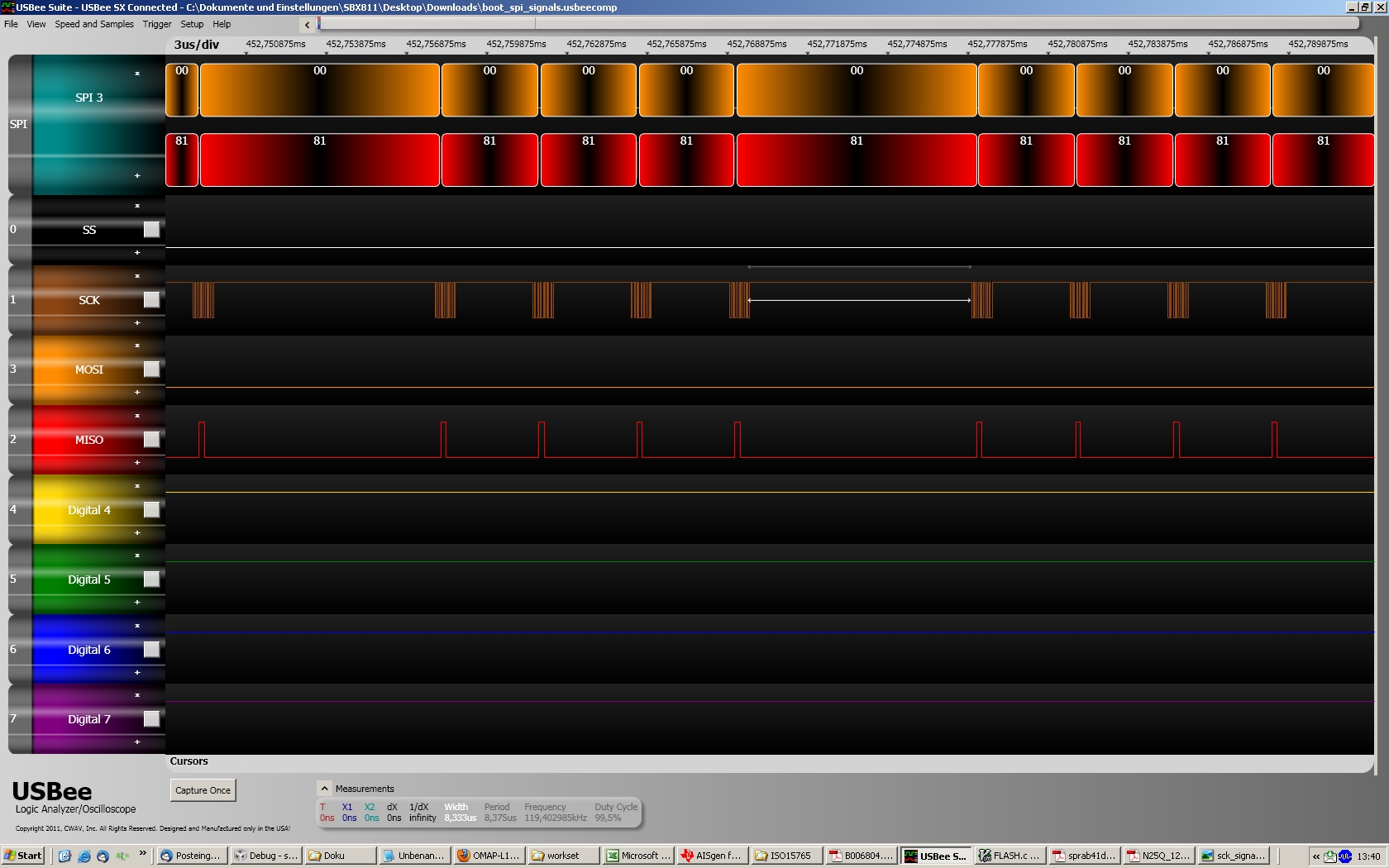
The loading of the image lasts for about 20-25 seconds. Normally I would expect that this is a matter of 3 seconds since I've configured the SPI clock to be 10 MHz. So I was wondering why and I've connected a logic analyzer to the SPI clock to analyze it and observed the signal curve in the attachment (the brown signal). You can see that after each 4 Bytes there is a pause (white double-arrow) of about 9 usecs and between each transfered byte within these 4 bytes a pause of about 3usecs. The configured frequency (10MHz) is only applied for the bits within one byte. Because of this also increasing the clock to 30 MHz doesn't help to boost things up, since the amount of the actual frequency (the 10 MHz) in the whole SPI transfer makes only about 20-30% (I would guess).
What is the reason for this? Did I missed any configuration? The optimal way is that SPI clock is driven without any pause (maybe only a small one between each SPI word transfer).
I've attached:
- a screenshot which shows the signal curve of the SPI clock during boot process
- my AISgen configuration file.
The ROM code version is D800K006 and a 20 MHz crystal is used to generate the controller clock.
Any help on this issue would be very appreciated. If you need any additional info, please let me know.
Thanks in advance,
Steve
Boot Mode=SPI1 Flash
Boot Speed=10
Flash Width=0
Flash Timing=3ffffffc
Configure Peripheral=True
Configure PLL0=True
Configure SDRAM=True
Configure PLL1=False
Configure DDR2=False
Configure LPSC=True
Configure Pinmux=True
Enable CRC=False
Specify Entrypoint=False
Enable Sequential Read=True
Use 4.5 Clock Divider=False
Use DDR2 Direct Clock=False
Use mDDR=True
ROM ID=2
Device Type=0
Input Clock Speed=20
Clock Type=0
PLL0 Pre Divider=1
PLL0 Multiplier=15
PLL0 Post Divider=1
PLL0 Div1=1
PLL0 Div3=3
PLL0 Div7=6
PLL1 Multiplier=20
PLL1 Post Divider=2
PLL1 Div1=1
PLL1 Div2=2
PLL1 Div3=3
Entrypoint=40008560
SDRAM SDBCR=4521
SDRAM SDTMR=31114620
SDRAM SDRSRPDEXIT=7
SDRAM SDRCR=30e
DDR2 PHY=0
DDR2 SDCR=0
DDR2 SDCR2=0
DDR2 SDTIMR=0
DDR2 SDTIMR2=0
DDR2 SDRCR=0
LPSC0 Enable=3+15+4+0+1+2+
LPSC0 Disable=
LPSC0 SyncRst=
LPSC1 Enable=3+0+21+
LPSC1 Disable=
LPSC1 SyncRst=
Pinmux=5:11000000+6:10111111+7:10000+8:11111111+9:11111111+11:11111111+12:11111111+13:80+3:401101+
App File String=D:\cc_workspace\DSPboot_FPGAboot\12_OMAPboot_SPIflash\Platform-B-Muster\ARMboot\Debug\ARMboot.out;D:\cc_workspace\DSPboot_FPGAboot\13_OMAP_FPGA_boot\FPGAboot\Debug\FPGAboot.out;D:\cc_workspace\DSPboot_FPGAboot\13_OMAP_FPGA_boot\upptest.mcs@0x41600000;
AIS File Name=D:\cc_workspace\DSPboot_FPGAboot\13_OMAP_FPGA_boot\FPGAboot.bin