This thread has been locked.

If you have a related question, please click the "Ask a related question" button in the top right corner. The newly created question will be automatically linked to this question.

[FAQ] AM3357: ADC AIN input for AM3357 (also applies to AM3352 , AM3354 , AM3356 ,AM3358 , AM3359)

Part Number: AM3357

Tool/software:

Hi team,

I am planning to input an analog signal to AM3357's AIN by dividing the voltage.
Was the constant of the voltage divider resistor OK with the constant shown in the figure?
I am wondering if I should add a voltage follower circuit because the voltage divider resistor value is large.
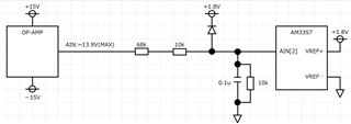
Best regards,

  • Hello,

    I have assigned your thread to one of our team members. Please note that this is a holiday week in India. Feel free to ping the thread next week if you do not get a response within a few business days.

    Regards,

    Nick

  • Hello takahiro higuchi

    Thank you for the query. 

    I am wondering if I should add a voltage follower circuit because the voltage divider resistor value is large.

    I would recommend implementing a voltage follower for optimal performance. The voltage follower amplifier power supply is recommended to be connected from the same power source that powers the processor ADC peripheral.

    Regards,

    Sreenivasa

  • Hello takahiro higuchi

    Please refer additional input i received from our power expert:

    They need to calculate the voltage error introduced when the ADC maximum input leakage current is drawn from the mid-point connection of the voltage divider.  They can decide if a buffer is needed once they understand the voltage shift on the voltage divider output due to input leakage current.

     Note: The ADC inputs are not fail-safe, so they should not apply any potential to the ADC input pins until the ADC power rail is valid.  This includes the analog input pins and both reference pins.  The two reference pins will not be a problem if the positive reference pin is connected to the same source as the ADC power rail and the negative reference pin is connected to VSS.

     The OP-AMP sourcing the analog input pin appears to be powered from a +/-15V supply which means its output could source a negative voltage. They need to ensure the OP-AMP never sources a potential than can cause the analog input to go outside the recommended operating range of ADC inputs.

     The reference inputs are analog inputs, which must be treated like high transient power supply rails. The negative reference pin is typically connected directly to the PCB ground plane along with all other VSS pins, and the positive reference pin is typically connected to the same power source that is used to power the ADC. This power source must be capable of providing at least 4mA of transient current. A high frequency decoupling capacitor should be located in the ball array on the back side of the PCB and connected directly between the two reference pins with vias such that the capacitor connection minimizes any loop inductance that would result in a voltage drop across the reference pins during a conversion.

    Regards,

    Sreenivasa

  • Hi team,

    Thanks for your answer.

    Could you please tell me the maximum leakage current of the ADC to calculate the voltage error?
    I didn't see any mention of the leakage current of the ADC in the datasheet, so I assume that the description of All other LVCMOS pins (VDDSHVx = 1.8 V; x = 1 to 6) would apply, is that correct?

    Best regards,

  • Hello takahiro higuchi

    Let me check with the expert and update you.

    regards,

    Sreenivasa