AM1808: EMAC(RMII) Communication Failure

Part Number: AM1808

Tool/software:

Hi Support Team,

Our customer has reported the following failure.

[Failure Overview]

App: Monitoring Monitor

Circumstance:
-Monitoring monitor to get a waveform is connected to the main monitor via a wired LAN and monitored centrally on the main monitor.
 In this case, there is a problem that the waveform on the main monitor is interrupted between 0.5s and 10s.

-There was no problem with the Ethernet's transmitted waveform, and the transmission was never stopped from the host side.

-When the transmission waveform was interrupted, the PHY (LAN8710AI)  inside the monitoring monitor was softly reset.

-The results of the evaluation revealed that when the transmission waveform was interrupted,
 the PHY (LAN8710AI) inside the monitoring monitor was soft reset.

-When we checked the cause of this reset, we found that it was due to a missing or unrecognized packet
 in the received packet. 

-We checked the waveforms of Ether and RMII, and did not find any significant missing waveforms
in Ether and RMII before the reset was issued.
 (Waveform quality could not be confirmed because the waveforms were observed
while the device was embedded in the equipment.)

-This model has been mass-produced for about 10 years and there had been no problem until now,
 However, 6 out of 10 units manufactured in 2023 and 13 out of 20 units manufactured
  in the most recent period had initial defects in the form of defective boards.
 
-We are currently investigating the cause of the problem, but based on the results of the current investigation,
 we believe that there may be some kind of failure in the RMII receiving side circuit of the AM1808 EMAC.
 The details are described following.

Results of our investigation:
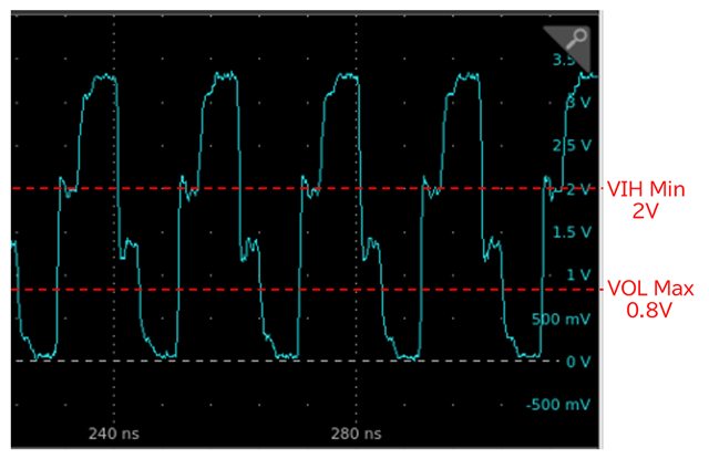
On this board, a damping resistor is placed near the RMII_MHZ_50_CLK (pin W18) of AM1808.
When the constant of this damping resistor is 10Ω, the problem occurs,
but when it is changed to 0Ω or 22Ω, the problem does not occur.


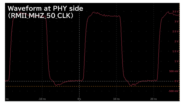
Waveforms of RMII_MHZ_50_CLK:
The waveforms were observed on the transmitter side (near the AM1808 W18 pin) and are therefore stepped.

The waveform observed at the receiving side (LAN8710AI) has no problem including setup/hold time.

RMII_MHZ_50_CLK is an input/output pin. If the waveform is stepped or
the transition time is 5ns or more (0.25P or more), is there a possibility that
a through-current flows through the input buffer at intermediate potentials, causing a problem?

We would appreciate it if you could point out any other points of concern.

Best Regards,
Kanae

  • I'm not familiar with how the RMII reference clock is implemented in the AM18108 device, but it appears to be operating as an output and input at the same time.

    There can be signal integrity problems if the AM1808 device is sourcing the clock to the PHY and the clock signal is also being looped back into the AM1808 device at the pin. This happens because the source end of an LVCMOS signal has a step function that occurs on the rising and falling edges with an amplitude that is a ratio of output buffer source impedance relative to the PCB trace impedance and has a duration that is 2x the PCB trace delay. You can see the step in each waveform you captured at the source end of the signal. The step is about mid-supply with a zero-ohm series termination resistor and moves further away from mid-supply as you increase the series termination resistor value. The AM1808 input buffer has a switching threshold near mid-supply. Therefore, you need to select a resistor value that moves the step away from the mid-supply region to minimize the risk of the AM1808 input buffer seeing multiple transitions and producing glitches on the internal RMII reference clock.

    Regards,
    Paul

  • Hi Paul,

    Thank you for your reply.

    I will share it with my customer.

    Best Regards,
    Kanae


  • Hi Paul,

    There are questions about your answer from our customer.


    Paul said;.
    I'm not familiar with how the RMII reference clock is implemented in the AM18108 device, but it appears to be operating as an output and input at the same time .

    Regarding the above, the RMII_REF_CLK is output from the AM1808 to the PHY in the register settings.
    What does it mean that it appears to be operating as an output and input at the same time .

    Paul said;.
    There can be signal integrity problems if the AM1808 device is sourcing the clock to the PHY and the clock signal is also being looped back into the AM1808 This happens because the source end of an LVCMOS signal has a step function that occurs on the rising and falling edges with an amplitude This happens because the source end of an LVCMOS signal has a step function that occurs on the rising and falling edges with an amplitude that is a ratio of output buffer source impedance relative to the PCB trace impedance and has a duration that is 2x the PCB trace delay.


    Regarding the above, I don't understand, the AM1808 is providing a 50MHz clock to the PHY and it does not seem to be feeding back the transmit clock to some pin of the AM1808.
    Is it simply an indication that there may be impedance between the AM1808 and the PHY and reflections caused by the PHY device?
    In fact, I suppose there is a step in the clock output from the CPU that is causing the reflections to occur.

    Paul said;
    You can see the step in each waveform you captured at the source end of the signal. The step is about mid-supply with a zero-ohm series termination resistor and moves further away from mid-supply as you increase the series termination resistor value.
    The AM1808 input buffer has a switching threshold near mid-supply. Therefore, you need to select a resistor value that moves the step away from the mid-supply region to minimize the risk of the AM1808 input buffer seeing multiple transitions and producing glitches on the internal RMII reference clock.


    Regarding the above, I believe the step occurs around 2V, which is away from the mid-supply region (1.65V) of the threshold supply voltage.
    On the other hand, the input H level is specified as min. 2V, so I assume that there is some kind of effect near 2V.
    I know it is important to eliminate steps, but I understand that both the rising and falling steps should be as close as possible to 1.65. Do you have a reference value?
    Also, is there any possibility of data loss in the RMII receive signal or MAC inside the AM1808 due to the clock step?

    We are not suspecting a defective device in this case, but rather experimentally changing the damping resistor from 10Ω to 22Ω in order to confirm the reason why the problem is improved.


    Best Regards,
    Kanae

  • The RMII_REF_CLK is being sourced by the AM1808 device. The IO cell associated with the RMII_REF_CLK output also contains an input buffer. The on-die pad that connects the IO buffer to the package terminal is also connected to the output of the output buffer and the input of the input buffer. So, the same clock that is sourcing the PHY is also being looped back at the on-die pad to source the internal RMII MAC circuits. This is done to help with receive data timing because looping the clock through the same output buffer and an input buffer with similar delay as the data input path allows the internal MAC RMII circuits to see the same clock output delay as the PHY and the same data input delay as the data being returned from the PHY during read operations.

    The unfortunate side-effect is the sensitivity to internal clock glitches when the voltage step that occurs on the source end of the transmission line is near the switching threshold. The resistance of the series termination resistor needs the be selected such that the step moves away from the mid-supply region. The series resistor needs to be located very close to the AM1808 pin with a very short trace connecting the series resistor to the AM1808 pin to be effective.

    Regards,
    Paul

  • Hi Paul,
    Thank you for your support.

    Paul said;
    The IO cell associated with the RMII_REF_CLK output also contains an input buffer. The on-die pad that connects the IO buffer to the package terminal is also connected to the output of the output buffer and the input of the input buffer. So, the same clock that is sourcing the PHY is also being looped back at the on-die pad to source the internal RMII MAC circuits.

    My apologies for my lack of understanding,
    which pin specifically does RMII_REF_CLK refer to?
    Are you referring to TX_CLK on the DP83822?
    Also, in which document section is the above mentioned information found?

    The customer's product in which the problem occurred has been on the market since 2013,
    and there have been no changes in the end user's operating environment, such as design changes
    or manufacturing process changes, since 2013.
    However, it is currently known that the defect has suddenly occurred in products manufactured in 2023
    and in recently manufactured products.
    The customer thinks that the stepped waveform of the clock has been occurring since 2013,
    and that the cause of the defect was originally latent in the RMII, and that the defect became apparent in a different lot of AM1808.

    Best Regards,
    Kanae

  • The IO associated with pin W18 on the AM1808 device is being used for the RMII_REF_CLK signal function.

    Please refer to the figure titled "EMAC Clocking Diagram" in the AM1808 TRM to see how the device can be configured to source SYSCLK7 to the EMAC and pin W18 when PINMUX15[3:0] is set to "1000", or an external 50MHz clock can be used to source the EMAC when PINMUX15[3:0] is set to "0000".  

    I was wrong when saying the clock signal is being looped through the IO call to the on-die pad and back into the device. It appears this older device was designed to send the clock directly to the EMAC via an internal path and also send it through the output buffer to the attached PHY via a separate parallel path when PINMUX15[3:0] is set to "1000".

    This clocking topology eliminates my previous concern of the PCB signal distortion causing a glitch on the internal EMAC clock.

    You should be looking at the clock signal quality near the attached PHY since it is important the clock being provided to the PHY is clean.

    The customers PCB may be violating the min setup and hold times on the AM1808 device if the PCB trace delays are too long. I suggest they focus on measuring data setup and hold margins relative the clock if the clock signal is clean near the PHY. See the table titled "Timing Requirements for EMAC RMII" in the device datasheet for the data setup and hold requirements.

    Regards,
    Paul

  • Hi Paul,

    Thank you for your reply.

    Please reply to the following simple confirmation from our customer.

    PINMUX15[3:0] is set to “1000” in AM1808 on the customer's board.
    The waveform of RMII_MHZ_50_CLK is shown below.
    The measurement point is near AM1808 W18 pin.

    The stepped waveform occurs around 2V, and the input H level is specified as min. 2V,
    so we assume that there is some kind of effect around 2V.

    If the following waveform is input to the input buffer of the IO cell of RMII_MHZ_50_CLK,
    is there a possibility of causing problems such as data corruption of RMII receive data inside AM1808?

    As mentioned in my first post, the waveform near PHY (RMII_MHZ_50_CLK) is confirmed to be OK as shown below.

    Confirmed that there is no problem including Setup/Hold.

    Of course, our customers will take countermeasures against this stepped waveform,
    but please answer the above question.

    Best Regards,
    Kanae

  • The AM1808 device was designed many years ago. The original design team is no longer available to ask questions. Therefore, I can only answer this question based on the implementation described in the device TRM. The TRM description seems to indicate there is two multiplexes controlled by the same PINMUX15[3:0] bits, where one multiplexer is used to select the EMAC clock source and the other selects the PHY clock source.

    The EMAC clock source is not being looped through the output buffer and input buffer if the internal clock connections are implemented as shown in the EMAC Clocking Diagram. I would not expect the step on the AM1808 end of the clock signal to cause a problem if the internal connection is implemented as drawn in the EMAC Clocking Diagram.

    There is a possibility the EMAC clock source is actually looped through the output buffer and input buffer to help with timing closure, and the diagram was drawn as shown trying to simplify the connection. The step voltage observed near the AM1808 pin is very likely to create internal glitches on the EMAC clock if the actual path is looped through the output buffer and input buffer and these steps occur between VIL and VIH. To be safe, I would suggest increasing the series termination resistor value until the step at the AM1808 pin increases above VIH on the rising edges and decreases below VIL on the falling edges.

    Regards,
    Paul

  • Hi Paul,

    Thank you for your support.
    I will share it with my customer.

    Best Regards,
    Kanae

  • Hi Paul,

    Thank you for your support.
    Here is an additional question from the customer.

    Paul said;
    The step voltage observed near the AM1808 pin is very likely to create internal glitches on the EMAC clock if the actual path is looped through the output buffer and input buffer and these steps occur between VIL and VIH. To be safe, I would suggest increasing the series termination resistor value until the step at the AM1808 pin increases above VIH on the rising edges and decreases below VIL on the falling edges.

    With regard to the above, is there any possibility of lot-to-lot variation in the threshold for glitching?

    Our customers understand that this variation is within the range of device specifications, but we would like to confirm that this phenomenon does not occur in lots prior to 2022, but in lots after 2023, there is a 60% probability of this issue occurring.

    Best Regards,
    Kanae