AM4372: How to implement DMA transmission between AM4372BZDNA60 and FPGA

Other Parts Discussed in Thread: AM4372, AM625
  • Hi Team.
  • 1、Currently, we plan to use AM4372BZDNA60 and FPGA to build a hardware system.
    Use the GPMC interface of the CPU (AM4372) to connect to NOR FLASH and communicate with the FPGA in a non-address data line multiplexing mode, with a maximum data bit of 16 bits.
    Transmit 8 data, 4 bytes each, using GPMC's DMA transmission. Using 8 DMA channels for transmission,Is this plan feasible?
  • 2、what is the maximum data transmission speed of DMA? What is the maximum FIFO buffer of each channel? What is the maximum memory that DMA can access? 512kb?
  • Thank you.

  • Hi Sheng,

    What OS do you use on AM4372, Linux or something else?

  • HI Bin Liu

    Does the user manual for the AM4372 provide specific details on the following content?

    9.1.3.3.5 GPMC DMA Requests
    The GPMC generates one DMA event, from GPMC (GPMC_DMA_REQ) to the eDMA: e_DMA_52.

    How does the GPMC interface utilize DMA to read data from the FPGA end?

  • e_DMA_52 is event 52 listed in AM437x TRM Table 10-24. It is the DMA event generated from GPMC module.

  • HI Bin Liu

    Can the GPMC interface support DMA transfers for 8 channels?

    EDMA has a total of 64 channels. When GPMC is reading data, can the data be allocated to 8 of these channels?

    Now it is necessary to read data from the FPGA through the GPMC interface. There are 8 packets of data, each packet containing 4 bytes. After GPMC receives the 8 packets of data, can 8 channels of DMA be configured to transfer the data?

  • Hi Sheng,

    No, only once DMA channel for GPMC, which is e_DMA_52 mentioned above. Once DMA channel can be configured to read 8x4 bytes of data from GPMC.

  • HI Bin Liu

    In EDMA, there are 64 directly mapped events corresponding to 64 channels one-to-one. Each event can only use a fixed channel, meaning that even if a particular event does not occur, the channel assigned to that event cannot be used by other events. Is this the correct understanding?

    How can the DMA transfer speed be confirmed? I did not see any information regarding this in the technical reference manual.

  • Hi Sheng,

    What OS do you use on AM4372, Linux or something else?

  • HI Bin Liu

    I'm currently not sure about which OS to use, just conducting hardware resource evaluations. What is the connection between the operating system and DMA? Please help confirm the previous question. Thank you.

  • Hi Sheng,

    First of all, I am a Linux buy, mostly comfortable in discussing the DMA usage in kernel device drivers, but I don't know all the eDMA module internals.

    In EDMA, there are 64 directly mapped events corresponding to 64 channels one-to-one. Each event can only use a fixed channel, meaning that even if a particular event does not occur, the channel assigned to that event cannot be used by other events. Is this the correct understanding?

    Yes, most of the DMA channels are one-to-one mapped to a particular source module, as shown in the TRM Table 11-24 and 11-25. But the Tables also list some channels which have "Open" source module, it means these channels can be mapped to different source modules.

    How can the DMA transfer speed be confirmed?

    The DMA throughput highly depends on the data package size. For example, the transfer speed would be greatly different in transferring from MMC than from UART. I don't have the DMA throughput report in Linux, but I am sure the DMA won't be the bottleneck when transferring from GPMC which max clk is 100MHz on AM437x, I believe.

  • HI Bin Liu

    Thank you for your response.

    My current requirement is to transition from the previous product, which used an SOC where the CPU and FPGA were integrated, and the internal FPGA transferred data to the CPU via DMA. I now intend to switch to the AM437x+FPGA mode. The current plan is to connect the AM437x and FPGA through the GPMC interface, with the AM437x internally transferring data to DDR via DMA.

    I found in the technical manual that the maximum clock for the GPMC interface is 100MHz, and the GPMC bandwidth should meet the requirements. However, the manual states that the maximum clock for TPCC and TPTC is 200MHz. Do I need to specifically focus on the DMA transfer speed, or is it sufficient to confirm the speed of the GPMC interface? What is the maximum buffer size when using DMA?

    Is there any technical documentation available for GPMC DMA configuration?

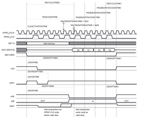
    As shown in the figure below. If we consider the read time of address bits and operate at the maximum frequency of 100MHz for GPMC, what is the maximum bandwidth that GPMC can achieve?

  • Hi Sheng,

    Do I need to specifically focus on the DMA transfer speed, or is it sufficient to confirm the speed of the GPMC interface?

    I tried to find an EDMA performance report, but didn't find any. However, I don't think you need to worry about EDMA performance on GPMC interface. The EDMA serves the entire AM437x system, including transferring data from DDR to DDR, which should be much faster than GPMC.

    What is the maximum buffer size when using DMA?

    AM437x DMA can do 3D transfer, each dimension is up to 64K. So the max buffer size would be 64K*64K*64K.

    f we consider the read time of address bits and operate at the maximum frequency of 100MHz for GPMC, what is the maximum bandwidth that GPMC can achieve?

    I am routing your query to our GPMC expert for comments.

  • HI Bin Liu

    Thank you for your response.

    I just learned that the software operating system required for the CPU is NORTi.

    The maximum clock for the AM43XX series GPMC interface is 100MHz, with a maximum data width of 16 bits, resulting in a data bandwidth of 100MHz x 2 bytes = 200MB/s. I calculated it this way. Is this calculation correct?
    Currently, there is a need to transfer LCD display data from the CPU to the FPGA. Based on the data size for different screen resolutions, VGA is approximately 100MB/s, SVGA is about 150MB/s, and XGA is around 250MB/s.
    It's possible that the bandwidth of the GPMC may not meet the requirements.
    Apart from connecting to the FPGA using the GPMC interface, can the AM43XX series connect to the FPGA through other interfaces as well?

  • Hi Sheng,

    The maximum clock for the AM43XX series GPMC interface is 100MHz, with a maximum data width of 16 bits, resulting in a data bandwidth of 100MHz x 2 bytes = 200MB/s. I calculated it this way. Is this calculation correct?

    It is roughly correct.

    It's possible that the bandwidth of the GPMC may not meet the requirements.
    Apart from connecting to the FPGA using the GPMC interface, can the AM43XX series connect to the FPGA through other interfaces as well?

    I cannot think of any other solution, but I am routing your query to our hardware expert for comments.

  • Hi Sheng,

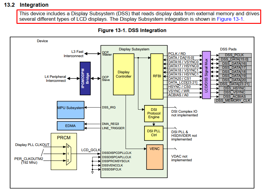
    The AM437x devices have a DSS module which is used to connect to display panels. So if it is possible to modify your FPGA to work with the DSS interface.

  • HI Bin Liu

    Sorry. I've been verifying CPU-related information these days, so I didn't reply promptly.

    1、Are you suggesting that the CPU connects to the LCD screen via the DSS interface instead of using the FPGA to connect to the LCD screen?

    2、Is it feasible to have a shared DDR for both the CPU and FPGA in a CPU+FPGA system design?

  • Hi Sheng,

    1、Are you suggesting that the CPU connects to the LCD screen via the DSS interface instead of using the FPGA to connect to the LCD screen?

    Yes.

    2、Is it feasible to have a shared DDR for both the CPU and FPGA in a CPU+FPGA system design?

    How FPGA can share DDR? Is the FPGA able to directly access DDR?

  • HI Bin Liu

    Due to the potential inadequacy of bandwidth using the GPMC interface, it is necessary to consider two alternative solutions:

    1. Whether the data drawing resources are sufficient when the DSS interface on the CPU side connects to the LCD screen (resolution 1024*768).
    2. Attaching a shared DDR3 to the CPU+FPGA system, where the address and data lines of both the CPU and FPGA connect to a single DDR3. Then, the CPU and FPGA determine DDR access using an SPI interface to manage contention. Are there any use cases from TI that implement this solution?

         Can you help me confirm solution 2? Thank you.

  • What is the frame rate at 1024x768? How did you concluded the dss interface is not sufficient for your project?

  • HI Bin Liu

    The frame rate for 1024x768 is 60Hz.

    I currently need to review the DSS interface to confirm if overlay display can be performed. The number of overlays required at the moment is 5 layers.

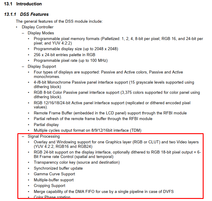
    Does the description inside the red box in the diagram below indicate that the AM437x can only achieve overlay of two layers?

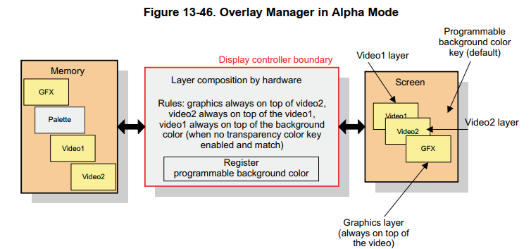
    Overlay and Windowing support for one Graphics layer (RGB or CLUT) and two Video layers  
    (YUV 4:2:2, RGB16 and RGB24)   How should this sentence be understood?

    How should this sentence be understood? "DSS reads display data from external memory and drives various types of LCD displays."

    What are the differences between the parallel bypass mode and RFBI mode of the LCD controller output? Since I need a 24-bit output, I cannot use the RFBI mode. In the bypass mode, can layering operations still be performed?

  • Hi Sheng,

    Does the description inside the red box in the diagram below indicate that the AM437x can only achieve overlay of two layers?

    Overlay and Windowing support for one Graphics layer (RGB or CLUT) and two Video layers  
    (YUV 4:2:2, RGB16 and RGB24)   How should this sentence be understood?

    Yes, one gfx layer plus two video payers, total 3 layers.

  • HI Bin Liu

    1、"What is the difference between one graphics layer (RGB or CLUT) and two video layers (YUV 4:2:2, RGB16, and RGB24)? Are these graphics and video layers existing side by side?"

    2、"I have reviewed the contents of the operation manual, and it seems that the GPMC function and DSS function cannot be used together because they share many multiplexed pins that can only support one function. However, I need to drive the LCD screen using the CPU while also using the GPMC interface to connect to the FPGA for data interaction."This may not be achievable.


  • Hi, Sheng,

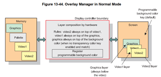
    1. Not side by side. All the 3 layers are overlayed.

    2. I thought your FPGA is to control the LCD. If it is connected to AM437x DSS, why is it still need to connect to GPMC?

  • Currently, there is a need to transfer LCD display data from the CPU to the FPGA. Based on the data size for different screen resolutions, VGA is approximately 100MB/s, SVGA is about 150MB/s, and XGA is around 250MB/s.

    Doesn’t this mean CPU transfer LCD display data to FPGA then FPGA drive the data to LCD?

    This is why I recommended to use AM437x DSS interface instead of GPMC.

  • HI Bin Liu

    1. Not side by side. All the 3 layers are overlayed.

    Is there any technical documentation available regarding the concept of one graphics layer (RGB or CLUT) and two video layers (YUV 4:2:2, RGB16, and RGB24)? I am unsure if our requirements align with this layering setup.

    We need to overlay display data from 5 layers to form one frame of display image.

    2. I thought your FPGA is to control the LCD. If it is connected to AM437x DSS, why is it still need to connect to GPMC?

    "I don't understand what you mean. Are you trying to convey that since AM437x is connected to the LCD via DSS, why is there a need for GPMC to connect to the FPGA?"

    "Our original design was a CPU+FPGA system, where the CPU handles the rendering of display data, then transfers this data to the FPGA for overlay design (5 layers) and driving the LCD screen. Since the current use of GPMC cannot meet the bandwidth requirements for displaying data, we want the CPU to handle rendering, layering, and driving the LCD display. However, our system still has other functions that require FPGA processing, and the FPGA still needs to transfer other data to the CPU. Therefore, we still need to retain the GPMC interface."

    But the DSS function and GPMC function of AM437x cannot be used simultaneously.

  • Hi Sheng,

    Is there any technical documentation available regarding the concept of one graphics layer (RGB or CLUT) and two video layers (YUV 4:2:2, RGB16, and RGB24)?

    Have you reviewed the device TRM section 13.3.3.4 "Overlay Support"?

    However, our system still has other functions that require FPGA processing, and the FPGA still needs to transfer other data to the CPU. Therefore, we still need to retain the GPMC interface."

    Okay, thanks for clarifying.

    But the DSS function and GPMC function of AM437x cannot be used simultaneously.

    I believe if you only use up to 12 address lines on GPMC (ball A19 would be used in both DSS and GPMC), you can use both DSS and GPMC in the same design.

  • HI Bin Liu

    "I have read section 13.3.3.4 'Overlay Support' of the device TRM. However, I still have a few questions."

    1、"What are the differences in composition between the graphics layer and the video layer? Why is it one graphics layer and two video layers instead of three graphics layers or three video layers?"

    2、"The overlay manager can be configured in two different modes:
    • Alpha mode (used only with the graphics layer with a source color key)
    • Normal mode (does not support alpha)"

    "The difference between the two modes is that in one, the graphics layer always stays above the video layer, and in the other, the graphics layer always stays below the video layer. How are these two modes chosen during development?""What differences will there be in the display effect?"

  • Hi Sheng,

    1、"What are the differences in composition between the graphics layer and the video layer? Why is it one graphics layer and two video layers instead of three graphics layers or three video layers?"

    From the applications perspective, they are just pipelines with different format support - graphics layer supports RBG or CLUT, while video layer supports YUV and RGB.

    How are these two modes chosen during development?"

    It should be controlled by DSS registers. (I am no longer supporting DSS, the last time I worked on DSS was more than 10 years ago.)

    What differences will there be in the display effect?

    It is all described in the TRM "Overlay Support" section.

    Here is an example of the use cases of Normal Mode, which hopefully can help understand:

    When implementing a video player which plays a movie in 16:9 ratio on an 4:3 monitor, the top and bottom of the monitor will be empty, the video player can fill it with a solid color (typically in black), this will be rendered on the graphics layer at the very back. Then the movie itself will be rendered on the video1 layer which takes the majority of the monitor and the closed caption will be rendered on the video2 layer on top of the movie, which typically is close to the bottom of the monitor.

  • Hi Sheng,

    BTY, do you consider AM62x devices instead of AM437x? AM62x just released a few years ago and has much more features than AM437x. You can check AM62x device datasheet to see if it fits better for your project.

    https://www.ti.com/product/AM625

  • HI Bin Liu

    That's a good suggestion. I'll check the AM625 specifications. However, I still need to prove the viability of the AM437x in this project.

  • Hi Sheng,

    the subject matter expert is out of the office this week (U.S. holidays), returning next week. Please allow some extra time for a response here.

    Regards, Andreas

  • Hi Andreas.

    OK. I am reviewing the previous response content. Thank you.

  • Hi Sheng,

    Please let me know if you still have any specific questions.