This thread has been locked.

If you have a related question, please click the "Ask a related question" button in the top right corner. The newly created question will be automatically linked to this question.

AM6421: DDR Read / Write issue

Part Number: AM6421
Other Parts Discussed in Thread: SYSCONFIG

Tool/software:

Hi,

         We have a custom Board with SOC AM6421 1GB K4A8G165WB-BCRC DDR.

         We are using mcu_plus_sdk_am64x_09_02_00_50   SDK.

We are testing the Hardware with example ddr_ecc_test_mcu_esm  from examples of SDK.

 We are facing the issue 
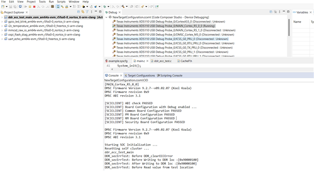
          The code is as below

When running the execution stops at line

testVal = gTest_Addr[0];

Back Ground:

   The same example work on our earlier Board which is 10 Layer Board and same DDR and SOC used.

 Our New Board is with 12 Layer and ICCSG interface changed to MII.

  We have checked the 12 layer Bare PCB Trace Lengths and track Impedance and found they are with in specified range.

  Can please help us to resolve the issue.

Thank you.

  • Hello Narashimha,

    Is the R5F core going into an abort when the execution stops? Can you pause the core and check if it is in an abort state? 

    Can you check the values of below registers when the execution stops?

    You can use the memory browser in CCS for checking these register values.

    Regards,

    Nihar Potturu. 

  • Hi Nihar,

       Thank You.

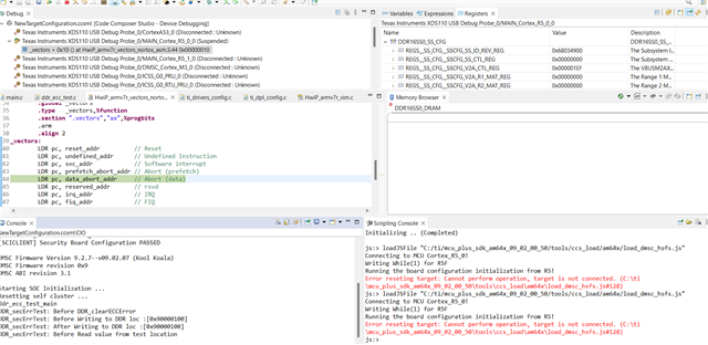
     Below are the screen shots as requested by you for the registers when the execution stops.

       When executions stops the program goes to abort state as attached.

    Please guide us what we should do next.

    Thank You

  • Hi Nihar,

           Any update on the DDR issue. Any other information you require.

    Thank You.

  • Hello Narasimha,

    Just to confirm, the same SW was working find on the old board but gives an abort in the new board right? And the DDR part and SoC are same in the new board as well. 

    I have assigned the thread to a HW expert so that he can comment further. There might be delay in response because of Thanksgiving holiday week in US. 

    Regards,

    Nihar Potturu. 

  • Hi Nihar,

       The same SW is working fine on old board, but gives data abort in the new board.

       The DDR and SOC part are same in both old board and new board.


       Can we except some quick response, because we have to give product delivery for customer

    . Thank You.

  • Might want to check if old silicon used AM6421A  versus  the (since Oct 2023)  AM6421B 

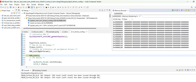
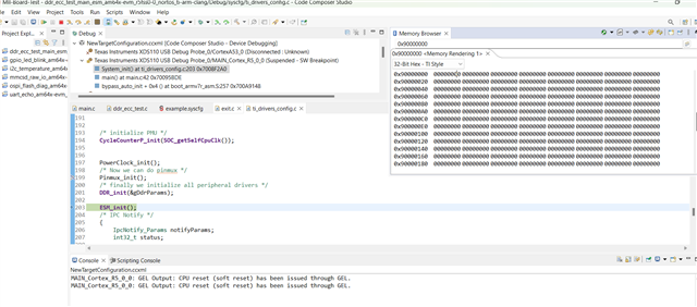
  • Before running the ECC test, can you do some basic checks on the memory by opening up a memory window and trying to peek/poke some values into DDR address space.  I would like to see if there are some bit errors without enabling the ECC.

    -Can you also send the output of the DDR register configuration file (both .syscfg and .h). 

    -Are you using VTT regulator?

    -Can you provide DDR register dump using the GEL script AM64x DDRSS Memory Debug->AM64x_DDRSS_CTL_PI_PHY_RegDump

    Regards,

    James  

  • Hi James,

       Thank you for the response.

    Are you using VTT regulator?   : Yes we are using.

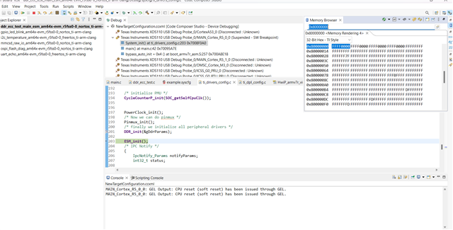
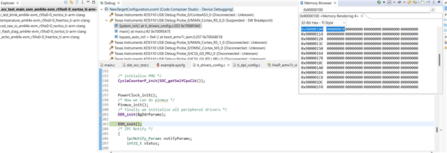
    Attached below is the Memory Window screen for Not working Board

    Attached below is the Register Dump for DDR.

    ddr_reg_nonworking.txt

    Sysconfig file used

    examplesyscfg.txt
    /**
     * These arguments were used when this file was generated. They will be automatically applied on subsequent loads
     * via the GUI or CLI. Run CLI with '--help' for additional information on how to override these arguments.
     * @cliArgs --device "AM64x" --package "ALV" --part "Default" --context "r5fss0-0" --product "MCU_PLUS_SDK_AM64x@09.02.00"
     * @versions {"tool":"1.20.0+3587"}
     */
    
    /**
     * Import the modules used in this configuration.
     */
    const ddr             = scripting.addModule("/drivers/ddr/ddr", {}, false);
    const ddr1            = ddr.addInstance();
    const esm             = scripting.addModule("/drivers/esm/esm", {}, false);
    const esm1            = esm.addInstance();
    const ipc             = scripting.addModule("/drivers/ipc/ipc");
    const debug_log       = scripting.addModule("/kernel/dpl/debug_log");
    const mpu_armv7       = scripting.addModule("/kernel/dpl/mpu_armv7", {}, false);
    const mpu_armv71      = mpu_armv7.addInstance();
    const mpu_armv72      = mpu_armv7.addInstance();
    const mpu_armv73      = mpu_armv7.addInstance();
    const mpu_armv74      = mpu_armv7.addInstance();
    const mpu_armv75      = mpu_armv7.addInstance();
    const mpu_armv76      = mpu_armv7.addInstance();
    const default_linker  = scripting.addModule("/memory_configurator/default_linker", {}, false);
    const default_linker1 = default_linker.addInstance();
    const general         = scripting.addModule("/memory_configurator/general", {}, false);
    const general1        = general.addInstance();
    const region          = scripting.addModule("/memory_configurator/region", {}, false);
    const region1         = region.addInstance();
    const section         = scripting.addModule("/memory_configurator/section", {}, false);
    const section1        = section.addInstance();
    const section2        = section.addInstance();
    const section3        = section.addInstance();
    const section4        = section.addInstance();
    const section5        = section.addInstance();
    const section6        = section.addInstance();
    const section7        = section.addInstance();
    const section8        = section.addInstance();
    const section9        = section.addInstance();
    const section10       = section.addInstance();
    const section11       = section.addInstance();
    
    /**
     * Write custom configuration values to the imported modules.
     */
    ddr1.$name                    = "CONFIG_DDR0";
    ddr1.eccEnableFlag            = true;
    ddr1.eccStart0                = 0x10000000;
    ddr1.eccEnd0                  = 0x10020000;
    ddr1.eccStart1                = 0x10020000;
    ddr1.eccEnd1                  = 0x10040000;
    ddr1.eccStart2                = 0x10040000;
    ddr1.eccEnd2                  = 0x10060000;
    ddr1.ddrConfigIncludeFileName = "drivers/ddr/v0/soc/am64x_am243x/board_ddrReginit_new303.h";
    
    esm1.$name                             = "CONFIG_ESM0";
    esm1.bClearErrors                      = true;
    esm1.esmNotifier.create(2);
    esm1.esmNotifier[0].$name              = "CONFIG_ESM_NOTIFY0";
    esm1.esmNotifier[0].errorNumber        = 6;
    esm1.esmNotifier[0].setIntrPriorityLvl = "LOW";
    esm1.esmNotifier[0].notify             = "DDR_secHandler";
    esm1.esmNotifier[1].$name              = "CONFIG_ESM_NOTIFY1";
    esm1.esmNotifier[1].errorNumber        = 69;
    esm1.esmNotifier[1].notify             = "DDR_dedHandler";
    
    ipc.r5fss0_1 = "NONE";
    ipc.r5fss1_0 = "NONE";
    ipc.r5fss1_1 = "NONE";
    ipc.m4fss0_0 = "notify";
    
    debug_log.enableUartLog        = true;
    debug_log.enableLogZoneInfo    = true;
    debug_log.uartLog.$name        = "CONFIG_UART_CONSOLE";
    debug_log.uartLog.intrEnable   = "DISABLE";
    debug_log.uartLog.UART.$assign = "USART0";
    
    const uart_v0_template  = scripting.addModule("/drivers/uart/v0/uart_v0_template", {}, false);
    const uart_v0_template1 = uart_v0_template.addInstance({}, false);
    uart_v0_template1.$name = "drivers_uart_v0_uart_v0_template0";
    debug_log.uartLog.child = uart_v0_template1;
    
    mpu_armv71.$name             = "CONFIG_MPU_REGION0";
    mpu_armv71.size              = 31;
    mpu_armv71.attributes        = "Device";
    mpu_armv71.accessPermissions = "Supervisor RD+WR, User RD";
    mpu_armv71.allowExecute      = false;
    
    mpu_armv72.$name             = "CONFIG_MPU_REGION1";
    mpu_armv72.size              = 15;
    mpu_armv72.accessPermissions = "Supervisor RD+WR, User RD";
    
    mpu_armv73.$name             = "CONFIG_MPU_REGION2";
    mpu_armv73.baseAddr          = 0x41010000;
    mpu_armv73.size              = 15;
    mpu_armv73.accessPermissions = "Supervisor RD+WR, User RD";
    
    mpu_armv74.$name             = "CONFIG_MPU_REGION3";
    mpu_armv74.accessPermissions = "Supervisor RD+WR, User RD";
    mpu_armv74.baseAddr          = 0x70000000;
    mpu_armv74.size              = 21;
    
    mpu_armv75.$name             = "CONFIG_MPU_REGION4";
    mpu_armv75.baseAddr          = 0x60000000;
    mpu_armv75.size              = 28;
    mpu_armv75.accessPermissions = "Supervisor RD, User RD";
    
    mpu_armv76.$name    = "CONFIG_MPU_REGION5";
    mpu_armv76.baseAddr = 0x80000000;
    mpu_armv76.size     = 31;
    
    default_linker1.$name = "memory_configurator_default_linker0";
    
    general1.$name        = "CONFIG_GENERAL0";
    general1.linker.$name = "TIARMCLANG0";
    
    region1.$name                               = "MEMORY_REGION_CONFIGURATION0";
    region1.memory_region.create(9);
    region1.memory_region[0].type               = "TCMA_R5F";
    region1.memory_region[0].$name              = "R5F_VECS";
    region1.memory_region[0].size               = 0x40;
    region1.memory_region[0].auto               = false;
    region1.memory_region[1].type               = "TCMA_R5F";
    region1.memory_region[1].$name              = "R5F_TCMA";
    region1.memory_region[1].size               = 0x7FC0;
    region1.memory_region[2].type               = "TCMB_R5F";
    region1.memory_region[2].$name              = "R5F_TCMB0";
    region1.memory_region[2].size               = 0x8000;
    region1.memory_region[3].$name              = "NON_CACHE_MEM";
    region1.memory_region[3].auto               = false;
    region1.memory_region[3].manualStartAddress = 0x70060000;
    region1.memory_region[3].size               = 0x8000;
    region1.memory_region[4].$name              = "MSRAM";
    region1.memory_region[4].auto               = false;
    region1.memory_region[4].manualStartAddress = 0x70080000;
    region1.memory_region[4].size               = 0x40000;
    region1.memory_region[5].type               = "FLASH";
    region1.memory_region[5].$name              = "FLASH";
    region1.memory_region[5].auto               = false;
    region1.memory_region[5].manualStartAddress = 0x60100000;
    region1.memory_region[5].size               = 0x80000;
    region1.memory_region[6].$name              = "USER_SHM_MEM";
    region1.memory_region[6].auto               = false;
    region1.memory_region[6].manualStartAddress = 0x701D0000;
    region1.memory_region[6].size               = 0x80;
    region1.memory_region[6].isShared           = true;
    region1.memory_region[6].shared_cores       = ["a53ss0-0","a53ss0-1","m4fss0-0","r5fss0-1","r5fss1-0","r5fss1-1"];
    region1.memory_region[7].auto               = false;
    region1.memory_region[7].manualStartAddress = 0x701D0080;
    region1.memory_region[7].size               = 0x3F80;
    region1.memory_region[7].$name              = "LOG_SHM_MEM";
    region1.memory_region[7].isShared           = true;
    region1.memory_region[7].shared_cores       = ["a53ss0-0","a53ss0-1","m4fss0-0","r5fss0-1","r5fss1-0","r5fss1-1"];
    region1.memory_region[8].auto               = false;
    region1.memory_region[8].manualStartAddress = 0x701D4000;
    region1.memory_region[8].size               = 0xC000;
    region1.memory_region[8].$name              = "RTOS_NORTOS_IPC_SHM_MEM";
    region1.memory_region[8].isShared           = true;
    region1.memory_region[8].shared_cores       = ["a53ss0-0","a53ss0-1","m4fss0-0","r5fss0-1","r5fss1-0","r5fss1-1"];
    
    section1.$name                        = "Vector Table";
    section1.load_memory                  = "R5F_VECS";
    section1.group                        = false;
    section1.output_section.create(1);
    section1.output_section[0].$name      = ".vectors";
    section1.output_section[0].palignment = true;
    
    section2.$name                        = "Text Segments";
    section2.load_memory                  = "MSRAM";
    section2.output_section.create(5);
    section2.output_section[0].$name      = ".text.hwi";
    section2.output_section[0].palignment = true;
    section2.output_section[1].$name      = ".text.cache";
    section2.output_section[1].palignment = true;
    section2.output_section[2].$name      = ".text.mpu";
    section2.output_section[2].palignment = true;
    section2.output_section[3].$name      = ".text.boot";
    section2.output_section[3].palignment = true;
    section2.output_section[4].$name      = ".text:abort";
    section2.output_section[4].palignment = true;
    
    section3.$name                        = "Code and Read-Only Data";
    section3.load_memory                  = "MSRAM";
    section3.output_section.create(2);
    section3.output_section[0].$name      = ".text";
    section3.output_section[0].palignment = true;
    section3.output_section[1].$name      = ".rodata";
    section3.output_section[1].palignment = true;
    
    section4.$name                        = "Data Segment";
    section4.load_memory                  = "MSRAM";
    section4.output_section.create(1);
    section4.output_section[0].$name      = ".data";
    section4.output_section[0].palignment = true;
    
    section5.$name                                   = "Memory Segments";
    section5.load_memory                             = "MSRAM";
    section5.output_section.create(3);
    section5.output_section[0].$name                 = ".bss";
    section5.output_section[0].palignment            = true;
    section5.output_section[0].output_sections_start = "__BSS_START";
    section5.output_section[0].output_sections_end   = "__BSS_END";
    section5.output_section[1].$name                 = ".sysmem";
    section5.output_section[1].palignment            = true;
    section5.output_section[2].$name                 = ".stack";
    section5.output_section[2].palignment            = true;
    
    section6.$name                                    = "Stack Segments";
    section6.load_memory                              = "MSRAM";
    section6.output_section.create(5);
    section6.output_section[0].$name                  = ".irqstack";
    section6.output_section[0].output_sections_start  = "__IRQ_STACK_START";
    section6.output_section[0].output_sections_end    = "__IRQ_STACK_END";
    section6.output_section[0].input_section.create(1);
    section6.output_section[0].input_section[0].$name = ". = . + __IRQ_STACK_SIZE;";
    section6.output_section[1].$name                  = ".fiqstack";
    section6.output_section[1].output_sections_start  = "__FIQ_STACK_START";
    section6.output_section[1].output_sections_end    = "__FIQ_STACK_END";
    section6.output_section[1].input_section.create(1);
    section6.output_section[1].input_section[0].$name = ". = . + __FIQ_STACK_SIZE;";
    section6.output_section[2].$name                  = ".svcstack";
    section6.output_section[2].output_sections_start  = "__SVC_STACK_START";
    section6.output_section[2].output_sections_end    = "__SVC_STACK_END";
    section6.output_section[2].input_section.create(1);
    section6.output_section[2].input_section[0].$name = ". = . + __SVC_STACK_SIZE;";
    section6.output_section[3].$name                  = ".abortstack";
    section6.output_section[3].output_sections_start  = "__ABORT_STACK_START";
    section6.output_section[3].output_sections_end    = "__ABORT_STACK_END";
    section6.output_section[3].input_section.create(1);
    section6.output_section[3].input_section[0].$name = ". = . + __ABORT_STACK_SIZE;";
    section6.output_section[4].$name                  = ".undefinedstack";
    section6.output_section[4].output_sections_start  = "__UNDEFINED_STACK_START";
    section6.output_section[4].output_sections_end    = "__UNDEFINED_STACK_END";
    section6.output_section[4].input_section.create(1);
    section6.output_section[4].input_section[0].$name = ". = . + __UNDEFINED_STACK_SIZE;";
    
    section7.$name                        = "Initialization and Exception Handling";
    section7.load_memory                  = "MSRAM";
    section7.output_section.create(3);
    section7.output_section[0].$name      = ".ARM.exidx";
    section7.output_section[0].palignment = true;
    section7.output_section[1].$name      = ".init_array";
    section7.output_section[1].palignment = true;
    section7.output_section[2].$name      = ".fini_array";
    section7.output_section[2].palignment = true;
    
    section8.$name                       = "User Shared Memory";
    section8.type                        = "NOLOAD";
    section8.load_memory                 = "USER_SHM_MEM";
    section8.group                       = false;
    section8.output_section.create(1);
    section8.output_section[0].$name     = ".bss.user_shared_mem";
    section8.output_section[0].alignment = 0;
    
    section9.$name                       = "Log Shared Memory";
    section9.load_memory                 = "LOG_SHM_MEM";
    section9.type                        = "NOLOAD";
    section9.group                       = false;
    section9.output_section.create(1);
    section9.output_section[0].$name     = ".bss.log_shared_mem";
    section9.output_section[0].alignment = 0;
    
    section10.$name                       = "IPC Shared Memory";
    section10.type                        = "NOLOAD";
    section10.load_memory                 = "RTOS_NORTOS_IPC_SHM_MEM";
    section10.group                       = false;
    section10.output_section.create(1);
    section10.output_section[0].$name     = ".bss.ipc_vring_mem";
    section10.output_section[0].alignment = 0;
    
    section11.$name                       = "Non Cacheable Memory";
    section11.load_memory                 = "NON_CACHE_MEM";
    section11.group                       = false;
    section11.type                        = "NOLOAD";
    section11.output_section.create(1);
    section11.output_section[0].$name     = ".bss.nocache";
    section11.output_section[0].alignment = 0;
    
    /**
     * Pinmux solution for unlocked pins/peripherals. This ensures that minor changes to the automatic solver in a future
     * version of the tool will not impact the pinmux you originally saw.  These lines can be completely deleted in order to
     * re-solve from scratch.
     */
    debug_log.uartLog.UART.RXD.$suggestSolution = "UART0_RXD";
    debug_log.uartLog.UART.TXD.$suggestSolution = "UART0_TXD";
    

    DDR Configuration file

    board_ddrReginit_new303.h

    Thank You.

  • Something doesn't seem right with the VREF training in the reg dump. 

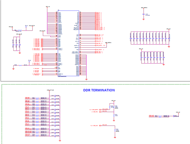
    -Can you send the DDR interface portion of the schematic?

    -ensure that the VTT regulator is enabled before the DDR4 is out of reset

    -is there a reason why you configured for 303MHz?  Did the other board work at 400MHz?

    -Please share the .syscfg file from the DDR register configuration tool.  The one you shared was for the SDK.

    -check all voltages on the board:

    Processor Voltage Rails:
    • VDDS_DDR = VDDS_DDR_C = 1.2V
    • VDDA_PLL1 = 1.8V (AM64x/AM243)

    Memory voltage rails:

    • VTT = 0.6V
    • DDR_VREFCA = 0.6V
    • DDR_VPP = 2.5V

    -How many boards have this issue?  From the regdump, it apprears DQ3 has an issue.  Can you send a regdump from a different board?

    -Also for comparison, a regdump from the working boards would be good as well

    Regards,

    James

  • Hi James,

    -is there a reason why you configured for 303MHz?  Did the other board work at 400MHz?

      Since the DDR was not working at 800MHz , so we configured it for 303MHz for debugging purpose.

      Our target is to work at 800MHz.

    -How many boards have this issue

      We have more than 8+ custom boards. And we have issue in all of them.

      Below are the measured Voltages.


    Supply Rail

    Required Value(V)

    Measured value(V)

    VDDS_DDR = VDDS_DDR_C

    1.2

    1.200

    VDDA_PLL1

    1.8

    1.803

    VTT = 0.6V

    0.6

    0.604

    DDR_VREFCA 

    0.6

    0.600

    DDR_VPP = 2.5V

    2.5

    2.505

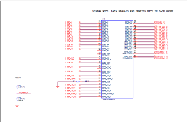
    the DDR interface portion of the schematic

    -DDR Registers of Working Board

    ddr-reg-workingboard.txt

    Configuration File generated from DDR sysconfig Tool.

    02355.board_ddrReginit.h

    Thank You.

  • One issue on the schematic:  DDR_RESET should be pulled low, not pulled high.  I don't think that is the solution to this problem, but it needs to be corrected.

    The working board regdump looks as expected.  So right now, the non-working board regdump indicates an assembly issue with DQ3.  So you will have to generate regdumps from the other boards to see what else could be the issue.  

    Also, i would recommend to use the latest DDR configuration tool v10.02: https://dev.ti.com/sysconfig/?product=Processor_DDR_Config&device=AM64x

    What was the conclusion of the memory browser tests?  Are you able to read/write locations in the memory browser before running the ECC test code?

    Regards,

    James 

  • Hi James,

               Thank you for the response.

      What was the conclusion of the memory browser tests?  Are you able to read/write locations in the memory browser before running the ECC test code?

      We have tried to access the DDR from two not working Boards from memory browser, Read and write to memory location has no impact.

       We tried to write some data to 0x80000000, but it does not affect anything.

       Below is the Register dump ,  memory browser and DDR configuration file used in the testing project form both the boards

       Board-1 Register Dump:

    ddr_reg_notworkingBoard1.txt

      Board-1 Memory Browser:

     Board-2 Register Dump:

    ddr_reg_notworkingBoard2.txt

      Board-1 Memory Browser:

    DDR Configuration file used:

    0143.board_ddrReginit.h

    At this point of time, we are using Industrial Communication SDK v9.2.0.15. So, we cannot move to SDK 10 as suggested by you.

    Thank You.

  • Hi James,

        Any Update on the DDR issue with the above information provided.

    Thank You

  • Hi James,

          Can we get any update on the DDR issue with the above information provided.

    Thank You

  • Hi James,

          Can we get any update on the DDR issue with the above information provided.

          Our customer is waiting for the solution We appreciate your quick response.

    Thank You

  • Hi James,


    Can we get any update on the DDR issue with the above information provided.

          Our customer is waiting for the solution We appreciate your quick response.

    Thank You

  • It appears from the register dump that the ECC is still enabled:

    R DDR16SS0_SS_CFG_REGS__SS_CFG__SSCFG_ECC_CTRL_REG 0x0000000B 0x00000117

    I would like to see the memory browser experiments performed without ECC enabled.  It should be a simple matter of changing that register to 0x0.  I'm not sure why the ECC would be enabled immediately after the DDR_Init().  Isn't ECC enabled sometime after that?

    Also, i checked both regdumps, and i still see an issue with DQ3 on in both regdumps.  The read eye training value does not match the rest of the data bus.  I'm also seeing a strange value for the Processor side VREF training for byte0.  It is a lot lower than the VREF for byte 1. 

    I don't have a good idea on why byte0 VREF is not training properly.  You previously said that you checked the layout between the working and non-working board.  Did anything change specifically in the DDR layout?  For example, routing layers, or reference planes. Are you using a different DDR4 device?  My only idea is that there is something wrong with the power distribution.  I saw that you checked voltages in a previous thread.  Can you take a more dynamic measurement on the 1.2V IO voltage with a scope, especially during DDR initialization.  Would like to ensure voltage is stable throughout the initialization.

    Regards,

    James


  • Hi James,

       "I'm not sure why the ECC would be enabled immediately after the DDR_Init().  Isn't ECC enabled sometime after that?"

        1)Before DDR_Init().  ECC Register showed ECC enable bit as 0.

       2) After DDR_Init().  ECC Register bit showed as 1.

       Would like to let you know that DDR_Init(). is changing ECC to 1.and it is a library api for us.


       Attached is the memory Browser information with ECC set to 0, after DDR _Init().We had written in to location 0x90000000 ~  0x90000040

      below pattern, we see a pattern of issue with the Memory.

     We have input below values at memory locations

     0x90000000 -  0x00000000

     0x90000020 -  0x11111111

     0x90000040 -  0x22222222

     0x90000060 -  0x33333333

     0x90000080 -  0x44444444  etc

    The other details had asked above will provide you shortly.

    Meanwhile would you be able to arrive at any conclusion, where the fault is.  from this memory pattern provided.

    Thank You

  • Narasimha,

    To disable ECC, you would have to go into sysconfig and disable it there by unchecking the box:

    The pattern you are showing indicates significant issues with DDR stability.  I'm not sure yet if there is an issue with the DDR configuration or a hardware issue, but since you had previous working hardware, i would suspect there is a hardware issue as i indicated earlier. 

    Please perform the hardware comparison and i will get back to you with more debug suggestions

    Regards,

    james