This thread has been locked.

If you have a related question, please click the "Ask a related question" button in the top right corner. The newly created question will be automatically linked to this question.

C6678 Decoupling on underside of BGA

Hi,

How do TI recommend the placing of decoupling capacitors on the underside of the C6678 0.8mm pitch BGA?

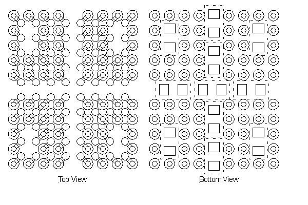
The hardware design guide says: "TI recommends placing decoupling capacitors immediately next to the BGA vias, using the interior BGA space and at least the corners of the exterior."  Of course this doesn't say how you recommend doing it!

The C6678 EVM does this by sharing through-hole vias between pads,  which leaves room to fit decoupling capacitors.  However, the EVM removes lots of vias.  In some cases, 9 BGA pads are tracked together on the component side and only two vias join this track to the power/gnd plane.

Is this recommended by TI?  It worries to me to see so many pads sharing a via.

cheers,

Richard

  • TI does recommend placing the bypass capacitors under the C6678 if possible and there are a number of strategies for placement.  The biggest problem associated with capacitor placement is the requirement of a via for every pad on the part.  Since the C6678 doesn't have any open rings this creates a full array of vias.  One strategy is to use blind vias to limit the vias that pass from the top to the bottom of the board.  A number of customers have split the board into a top half and a bottom half using vias that are limited to one half to route many of the signals allowing capacitors to be placed directly under the C6678. 

    If a blind via strategy is not an option 0402 capacitor cannot be place directly under the part due to the spacing of the vias.  You may be able to place 0201 capacitors depending on the drill size used for your vias.  One strategy that has been used is to fan the via connections away from the center of the part creating an open cross which can be used to place capacitors.

     This will allow a line of capacitors to be placed in a cross pattern down the center of the part.  The balance of capacitors will either have to be place around the edge of the part or interspersed under the part with a minimum number of pads sharing vias.