This thread has been locked.

If you have a related question, please click the "Ask a related question" button in the top right corner. The newly created question will be automatically linked to this question.

[FAQ] AM6442: How does LVCMOS buffer behavior

Part Number: AM6442

Tool/software:

Hi

I got an additional question to

   https://e2e.ti.com/support/processors-group/processors---internal/f/processors---internal-forum/1435716/am6442-specification-of-output-voltage-of-lvcmos


The summary of the above is


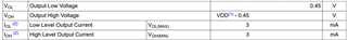
The customer is trying to use the LVCMOS output pin with 1.8VMODE, but the maximum vol value is 0.45V (IOL = 3mA), which is a high specified value, and the design does not work if the electrical characteristics are interpreted as it is.


Then I got the answer as the below.

The max limit defined for VOL is valid as long as the IOL is less than 3mA, and the min limit defined for VIH is valid as long as the IOH is less than 3mA.

The datasheet is saying the output buffer is able to sink current up to the min IOL current of 3mA and the low-level output voltage will remain less than the max value of 0.45V defined for VOL, and the output buffer is able to source current up to the min IOH current of 3mA and the high-level output voltage will remain greater than the min value of (VDD - 0.45V) defined for VOH.


I understand that TI's guaranteed values are above.

How does a circuit act as a LVCMOS buffer?

If an external PD resistor or input buffer is connected and the low-side FET is turned on while AM64 is output low, will the current not drive?

  • The output buffer will source current from the respective VDD IO power rail to the external connections when driven high, or sink current from the external connections to VSS when driven low. The signal voltage will depend on the source current or sink current. The only data point we define in the datasheet is for current up to 3mA, where the signal voltage will remain less than the max VOL value of 0.45V as long as the sink current is less than 3mA, and the signal voltage will remain greater than the min VOH value of (VDD - 0.45V) as long as the source current is less than 3mA. The internal voltage dropped across the output buffer will decrease as the current decreases. A typical LVCMOS input buffer only has a few uA of input leakage current that needs to be driven by the output buffer to hold a valid logic state. There is a good chance external pulls, internal pulls, or combinations of external and internal pulls will present a much larger load than all attached input buffers.

    We provide an IBIS model of the output buffer that can be used to determine the resulting signal voltage for operating conditions not defined in the datasheet.

    You will need to create a simulation environment that represents your specific implementation and use the IBIS files of each device to determine the steady-state signal voltage for your specific system implementation if you are connecting a device that requires a logic high signal voltage that is greater than the min VOH value of (VDD - 0.45V) or a logic low signal voltage that is less than the max VOL value of 0.45V.

    Regards,
    Paul

  • Thank you very much for such a detailed!!