Because of the Thanksgiving holiday in the U.S., TI E2E™ design support forum responses may be delayed from November 25 through December 2. Thank you for your patience.

AM620-Q1: About OSPI Flash sysconfig settings (protocol, input clock frequency)

Genius 5785 points
Part Number: AM620-Q1

Tool/software:

Hi experts,

My customer is using AM62x and wants to set OSPI Flash and OSPI Flash Boot in CCS, but there are some questions about each setting.

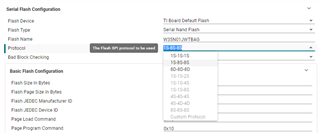
Q1. In .syscfg, Serial Flash Configuration supports three types of Protocol: "1S-1S-1S", "1S-8S-8S", and "8D-8D-8D". However, in AM62x technical reference, OSPI Boot supports "1S-1S-8S Only", and Serial NAND Boot supports "1S-1S-1S ~ 1S-1S-8S", so the only one that matches this is Serial NAND Boot's "1S-1S-1S".
Does this Protocol not have to match the Boot Protocol specification?
Should I select "1S-8S-8S" for Protocol, as per the Serial NAND Flash Boot example in SDK?
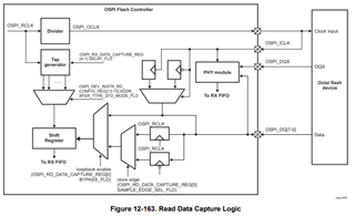
Q2. In the OSPI Driver Configuration of .syscfg, where should I refer to when setting the Input Clock Frequency (Hz) and Input Clock Divider settings? Do the settings refer to the OSPI_RCLK and Divider of the QSPI Flash Controller in the figure below?
Q3. In the Serial NAND Flash Boot example in the SDK example, the Input Clock Frequency (Hz) is "166666666" and the Input Clock Divider is "4". Why are these settings set to these values?
(Is it because the maximum clock frequency in SDR mode of the W35N01JWTBAG is 166MHz? In that case, shouldn't the settings be the OSPI_RCLK and Divider of the OSPI Flash Controller?)

Best regards,
O.H

  • Hello Otomo,

    Thanks for your detailed questions.

    Allow me sometime to provide responses for three of your questions.

    Regards,

    Vaibhav

  • Here is a detailed explanation on your questions:

    Q1. In .syscfg, Serial Flash Configuration supports three types of Protocol: "1S-1S-1S", "1S-8S-8S", and "8D-8D-8D". However, in AM62x technical reference, OSPI Boot supports "1S-1S-8S Only", and Serial NAND Boot supports "1S-1S-1S ~ 1S-1S-8S", so the only one that matches this is Serial NAND Boot's "1S-1S-1S".
    Does this Protocol not have to match the Boot Protocol specification?
    Should I select "1S-8S-8S" for Protocol, as per the Serial NAND Flash Boot example in SDK?

    So currently in our SDK offering for a:

    1. NOR Flash: The best performance supported is 8D-8D-8D mode, with 166 MHz, Clock Divider 8, DMA enabled, Phy enabled.
    2. NAND Flash: The best performance supported is 1S-8S-8S mode, with 166 MHz, Clock Divider 4, DMA enabled, Phy Enabled

    Q2. In the OSPI Driver Configuration of .syscfg, where should I refer to when setting the Input Clock Frequency (Hz) and Input Clock Divider settings? Do the settings refer to the OSPI_RCLK and Divider of the QSPI Flash Controller in the figure below?

    RCLK is the Frequency which you specify and the divider is effective only in certain scenarios.

    Assume your frequency is 166 MHz, and divider is 4. So when:

    1. Phy is disabled: All OSPI operations, read/write/erase happens at a frequency of 166/4 ~ 40 MHz.
    2. Phy is enabled: All OSPI operations, except read, happens at 40 MHz, only the read operation happens at 166 MHz. So to summarize, when Phy is enabled, the read operation happens at 166 MHz as the clock divider is bypassed for faster reads, but the remaining operations like write and erase would still happen at 40 MHz.
    Q3. In the Serial NAND Flash Boot example in the SDK example, the Input Clock Frequency (Hz) is "166666666" and the Input Clock Divider is "4". Why are these settings set to these values?

    As mentioned this is what we currently support, plus for SDR, we always have a clock divider value of 4.

    I hope this answers all your doubts.

    Regards,

    Vaibhav