TDA4VM: Can not access PCIE2_DAT0

Part Number: TDA4VM

Tool/software:

Hi TI,

we have currently an issue with PCIE2_DAT0 on TDA4. We are using ti-uboot-2023.04 to bring the TDA4 until u-boot stage, which then loads and starts the firmware for mcu2-0.

The pcie module index 2 is configured to access memory of another board with TDA4 via PCIE2_DAT0 region.

The issue is, that I can not access PCIE2_DAT0 region from mcu2-0. Following summarizes what I have tried so far:

1. PCIE2_DAT0 memory is located within 48-bit address space. (0x4400000000)
The RAT unit of mcu2-0 is configured to map this memory region (0x4400000000) into ARMSS_RAT_REGION2 address range (0x10000000)
I connect CCS to mcu2-0, and use the memory browser to read from the mapped memory region (0x10000000).

Result: I get "?" in Memory Browser view and it looks that the TDA4 has crashed.

CCS Output: MAIN_Cortex_R5_0_0: Error: (Error -1170 @ 0x0) Unable to access the DAP. Reset the device, and retry the operation. If error persists, confirm configuration, power-cycle the board, and/or try more reliable JTAG settings (e.g. lower TCLK). (Emulation package 20.0.0.3178)
MAIN_Cortex_R5_0_0: Unable to determine target status after 20 attempts
MAIN_Cortex_R5_0_0: Failed to remove the debug state from the target before disconnecting.  There may still be breakpoint op-codes embedded in program memory.  It is recommended that you reset the emulator before you connect and reload your program before you continue debugging

2. Try to avoid any RAT configuration issues and using the A72 core to peek into PCIE2_DAT0 region:
I connect CCS to a72 and use memory browser to read from memory region 0x4400000000.
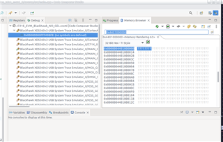
It just shows "?" (cannot read from that address) but this time, the TDA4 is not crashing like from R5.

Note: The "Memory View" is set to "CPU Memory View".

3. Same as 2, but this time I set Memory View of Memory Browser to "Physical Memory View".
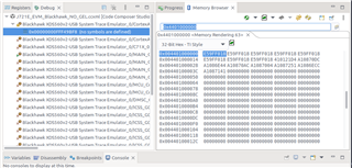
Now I can see the data from the other board. (It works!)

The conclusion for me is, that the PCI configuration/access in general is working. But there is an general issue of accessing PCIE2_DAT0.

Can you please help me here? Our final goal is to access it from mcu2-0.

Thank you and best regards,
Thomas

  • Hi Thomas,

    As a disclaimer, TI does not have software support for PCIe RTOS driver, and thus, no support for PCIe on R5F. TI only supports Linux driver hosted on the A72 core. So, although what you are attempting is not a full blown out driver implementation, it is uncharted territory. 

    You have mentioned U-Boot is in play, but when is the PCIe memory space accessed in both the case of using MCU2-0 to peek and A72 to peek at memory? Is it accessed in both cases after Linux has booted up and initialized the PCIe module, or is it stopped in U-Boot before going into Linux?

    Regards,

    Takuma

  • Hi Takuma,

    thank you for your reply. Yes, I am aware of that. I'm not asking for support of how to configure the pcie module correctly, that a pci link is established between two pci modules (this is working).

    I think there is some issue on the path between any core (A72, mcu2-0) and PCIE2_DAT0. For that I need support.

    To answer your question: In all three scenarios, following is happening:

    1. u-boot is booting
    2. u-boot loads mcu2-0 firmware and starts mcu2-0 with it
    3. At this point, A72 is not doing anything. No linux is booted. It just idles in u-boot environment.
    4. mcu2-0 firmware initializes and configures serdes & pcie module
    5. mcu2-0 firmware establishes successfully a data link of pcie module with another board. (LTSSM reaches L0)
    6. At this point, I start to try to access PCIE2_DAT0 with CCS Memory Browser as described in my first post.

    As my 3. scenario in the first post shows, I can read/write successfully on PCIE2_DAT0 with memory browser (connected to A72), but with "physical memory view". So it's not a general issue with the pci module configuration.

    Therefore I think it's somehow the path between a core and PCIE2_DAT0.

    I'm not an TDA4 expert, but I guess that

    1. MPU configuration of R5
    2. RAT configuration of R5
    3. Firewall configuration
    4. QoS configuration

    are potential issues. Propably even more, which I simply dont know yet.

    My quick test, to simply use the A72 for PCIE2_DAT0 access has the background to eliminate 1 and 2 from that list.
    I hope you can help me here to solve that issue. I also hope that there is no general "silicon issue" which prevents the access.
    Thank you and best regards,
    Thomas
  • Hi Thomas,

    For Linux, there is some mechanism to define some flags for the memory space like in this documentation: https://elinux.org/Device_Tree_Usage 

    I am not sure how this is handled for your code, but perhaps this is missing?

    Regards,

    Takuma

  • Hi Takuma,

    do you mean the phy.high bits in your screenshot? They are handled in the pci driver and the pci module gets correctly configured from my point of view.

    Are we here on the same page? How does the linux use this information to configure QoS (Chapter 3.3.2 of TDA4 TRM SPRUIL1B), or Firewall (Chapter 3.3.4 / 3.4 same document), which may influences the data access from mcu2_0 to PCIE2_DAT0 ?

    Regards,
    Thomas

  • Hi Thomas,

    Yes, mainly phys.hi bit flags like prefetchable and space code, as this can affect cache. One suspicion I have is issue with cache where the data in CPU cache is not invalidated. If physical memory has changed due to an external device writing data, but the core is not reading the correct values, then it could be due to cache coherency issues.

    As for firewalls, unless the device is a HS-FS (High Security Field Securable) device that has SoC firewalls enabled explicitly, then it should be no concern. Most folks use the general purpose GP device that has all firewalls disabled or HS-FS device where the security is not enforced. If you are using a HS-FS that has been burned with a key, and that is the cause for your concern with firewalls, then we can pursue this path.

    As for QoS, this is mainly used for giving priority to certain data transactions, useful for when there is a lot of activity on the entire SoC and causing some real time data transactions like display/GPU to have glitches due to DDR bandwidth issues and whatnot. It also can affect ASEL which affects cache coherency.

    Regards,

    Takuma

  • Hi Takuma,

    One suspicion I have is issue with cache where the data in CPU cache is not invalidated. If physical memory has changed due to an external device writing data, but the core is not reading the correct values, then it could be due to cache coherency issues.

    I don't think I have a cache related problem (yet). I simply can not read from that memory address. I do not have a problem that the data (which I can not read) seems to be wrong. I can not read the memory at all.

    Am I here on the wrong path?

    Most folks use the general purpose GP device that has all firewalls disabled or HS-FS device where the security is not enforced.

    We are using the GP device. My hope was that it could be a firewall issue, which is a solvable problem.
    Anyways, my next idea was, to use the firewall as a "logger". To see if the memory read request from the cpu actually reaches the interconnect until the pcie2 module.

    Can you help me with that?

    As for QoS, this is mainly used for giving priority to certain data transactions, useful for when there is a lot of activity on the entire SoC and causing some real time data transactions like display/GPU to have glitches due to DDR bandwidth issues and whatnot.

    Back in 2002 I had a problem, that after a PSDK Update (v07 to v08) I could not access some DRU register anymore. (https://e2e.ti.com/support/processors-group/processors/f/processors-forum/1179834/tda4vm-cannot-access-compute_cluster0_dru_queue-from-mcu2_0-after-u-boot-upgrade-7-3-to-8-x)

    After a lot of investigation it turned out that QoS settings caused it. At least that it what I understood from the discussion with Brijesh Jadav.

    TI registered this issue as LCPD-34679. This is the reason, why also the QoS comes as possible reason for that kind of issue in my mind.

    What do you think about that?

    Regards,
    Thomas

  • Hi Thomas,

    Am I here on the wrong path?

    No, I do not think so. However, the way the problem was described (aka, physical memory has actual data, but cores cannot access data) is very similar to cache issue. 

    Can you help me with that?

    Not with using firewall with logging. Firewall only sends out an exception log when it is enabled.

    What do you think about that?

    Maybe. I was not aware of QoS affecting in this way, but I am aware that in more recent SDK versions the QoS registers that are getting touched by that previous issue is being modified to solve bandwidth issue between DDR to display pipeline. You can try to apply patches to the NAVSS north bridge registers as an experiment, since it looks like the past issue was due to setting the register for realtime causing access to not happen:

    From e6fa2b99343909adb60d9eaa766afc36d3ce3654 Mon Sep 17 00:00:00 2001
    From: Neha Malcom Francis <n-francis@ti.com>
    Date: Tue, 18 Jul 2023 13:21:00 +0530
    Subject: [PATCH] arm: mach-k3: j721e: Drop write to NB0 threadmap
    
    Drop write to NAVSS0 NB0 threadmap register. Writing to bit 1 of this
    register makes DRU registers inaccessible. Capture/display paths are not
    affected.
    
    Signed-off-by: Neha Malcom Francis <n-francis@ti.com>
    ---
     arch/arm/mach-k3/j721e_init.c | 1 -
     1 file changed, 1 deletion(-)
    
    diff --git a/arch/arm/mach-k3/j721e_init.c b/arch/arm/mach-k3/j721e_init.c
    index c3371d4969..ec0d976691 100644
    --- a/arch/arm/mach-k3/j721e_init.c
    +++ b/arch/arm/mach-k3/j721e_init.c
    @@ -196,7 +196,6 @@ void do_dt_magic(void)
     void setup_navss_nb(void)
     {
             /* Map orderid 8-15 to VBUSM.C thread 2 (real-time traffic) */
    -        writel(2, NAVSS0_NBSS_NB0_CFG_NB_THREADMAP);
             writel(2, NAVSS0_NBSS_NB1_CFG_NB_THREADMAP);
     }
     
    -- 
    2.34.1

    Regards,

    Takuma

  • Hi Takuma,

    Not with using firewall with logging. Firewall only sends out an exception log when it is enabled.

    My idea was, to use the firewalls as "logging device". For example to enable PCIE2_DAT0 firewall, to verify if there is any activity when the mcu2_0 executes a read access, or see the difference when the read access of A72 works/works not.

    And then following the "access path" from mcu2_0 to PCIE2_DAT0 "backwards" to narrow down the issue.
    This is my last idea I have, to get at a feet into the door to somehow diagnose the problem.

    Regarding the patch, I will try this today and come back to you with the result.

    Update: I checked the patch.

    The line
     writel(2, NAVSS0_NBSS_NB0_CFG_NB_THREADMAP);
    is already removed in our u-boot.

    Regards,
    Thomas

  • Hi Thomas,

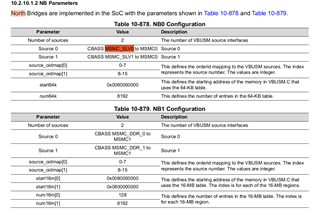
    Could you also confirm whether NB1 line is removed? I see NB0 is for MSMC0 and NB1 is for DDR based on the TRM.

    As for firewall, I am not too savvy in this area. But, I do see you have opened up a separate thread for this, and a colleague of mine who is more knowledgeable in this area has been notified (although, there will be a delay in his response due to being out of office): https://e2e.ti.com/support/processors-group/processors/f/processors-forum/1449673/tda4vm-inconsistency-with-ti_sci-firewall-configuration?tisearch=e2e-sitesearch&keymatch=firewall#

    And based on this other forum thread, I assume you may have found the TISCI documentation for firewall, but linking here just in case otherwise: https://software-dl.ti.com/tisci/esd/latest/2_tisci_msgs/security/firewall_api.html

    Regards,

    Takuma

  • Hi Takuma,

    Could you also confirm whether NB1 line is removed? I see NB0 is for MSMC0 and NB1 is for DDR based on the TRM.

    The NB1 line is not removed. For completeness, I paste the whole j721e_init.c file here:

    // SPDX-License-Identifier: GPL-2.0+
    /*
     * J721E: SoC specific initialization
     *
     * Copyright (C) 2018-2019 Texas Instruments Incorporated - http://www.ti.com/
     *	Lokesh Vutla <lokeshvutla@ti.com>
     */
    
    #include <common.h>
    #include <init.h>
    #include <spl.h>
    #include <asm/io.h>
    #include <asm/armv7_mpu.h>
    #include <asm/arch/hardware.h>
    #include <asm/arch/sysfw-loader.h>
    #include "common.h"
    #include <asm/arch/sys_proto.h>
    #include <linux/soc/ti/ti_sci_protocol.h>
    #include <dm.h>
    #include <dm/uclass-internal.h>
    #include <dm/pinctrl.h>
    #include <dm/root.h>
    #include <fdtdec.h>
    #include <mmc.h>
    #include <remoteproc.h>
    
    #ifdef CONFIG_K3_LOAD_SYSFW
    struct fwl_data cbass_hc_cfg0_fwls[] = {
    #if defined(CONFIG_TARGET_J721E_R5_EVM)
    	{ "PCIE0_CFG", 2560, 8 },
    	{ "PCIE1_CFG", 2561, 8 },
    	{ "USB3SS0_CORE", 2568, 4 },
    	{ "USB3SS1_CORE", 2570, 4 },
    	{ "EMMC8SS0_CFG", 2576, 4 },
    	{ "UFS_HCI0_CFG", 2580, 4 },
    	{ "SERDES0", 2584, 1 },
    	{ "SERDES1", 2585, 1 },
    #elif defined(CONFIG_TARGET_J7200_R5_EVM)
    	{ "PCIE1_CFG", 2561, 7 },
    #endif
    }, cbass_hc0_fwls[] = {
    #if defined(CONFIG_TARGET_J721E_R5_EVM)
    	{ "PCIE0_HP", 2528, 24 },
    	{ "PCIE0_LP", 2529, 24 },
    	{ "PCIE1_HP", 2530, 24 },
    	{ "PCIE1_LP", 2531, 24 },
    #endif
    }, cbass_rc_cfg0_fwls[] = {
    	{ "EMMCSD4SS0_CFG", 2380, 4 },
    }, cbass_rc0_fwls[] = {
    	{ "GPMC0", 2310, 8 },
    }, infra_cbass0_fwls[] = {
    	{ "PLL_MMR0", 8, 26 },
    	{ "CTRL_MMR0", 9, 16 },
    }, mcu_cbass0_fwls[] = {
    	{ "MCU_R5FSS0_CORE0", 1024, 4 },
    	{ "MCU_R5FSS0_CORE0_CFG", 1025, 2 },
    	{ "MCU_R5FSS0_CORE1", 1028, 4 },
    	{ "MCU_FSS0_CFG", 1032, 12 },
    	{ "MCU_FSS0_S1", 1033, 8 },
    	{ "MCU_FSS0_S0", 1036, 8 },
    	{ "MCU_PSROM49152X32", 1048, 1 },
    	{ "MCU_MSRAM128KX64", 1050, 8 },
    	{ "MCU_CTRL_MMR0", 1200, 8 },
    	{ "MCU_PLL_MMR0", 1201, 3 },
    	{ "MCU_CPSW0", 1220, 2 },
    }, wkup_cbass0_fwls[] = {
    	{ "WKUP_CTRL_MMR0", 131, 16 },
    };
    #endif
    
    static void ctrl_mmr_unlock(void)
    {
    	/* Unlock all WKUP_CTRL_MMR0 module registers */
    	mmr_unlock(WKUP_CTRL_MMR0_BASE, 0);
    	mmr_unlock(WKUP_CTRL_MMR0_BASE, 1);
    	mmr_unlock(WKUP_CTRL_MMR0_BASE, 2);
    	mmr_unlock(WKUP_CTRL_MMR0_BASE, 3);
    	mmr_unlock(WKUP_CTRL_MMR0_BASE, 4);
    	mmr_unlock(WKUP_CTRL_MMR0_BASE, 6);
    	mmr_unlock(WKUP_CTRL_MMR0_BASE, 7);
    
    	/* Unlock all MCU_CTRL_MMR0 module registers */
    	mmr_unlock(MCU_CTRL_MMR0_BASE, 0);
    	mmr_unlock(MCU_CTRL_MMR0_BASE, 1);
    	mmr_unlock(MCU_CTRL_MMR0_BASE, 2);
    	mmr_unlock(MCU_CTRL_MMR0_BASE, 3);
    	mmr_unlock(MCU_CTRL_MMR0_BASE, 4);
    
    	/* Unlock all CTRL_MMR0 module registers */
    	mmr_unlock(CTRL_MMR0_BASE, 0);
    	mmr_unlock(CTRL_MMR0_BASE, 1);
    	mmr_unlock(CTRL_MMR0_BASE, 2);
    	mmr_unlock(CTRL_MMR0_BASE, 3);
    	mmr_unlock(CTRL_MMR0_BASE, 5);
    	if (soc_is_j721e())
    		mmr_unlock(CTRL_MMR0_BASE, 6);
    	mmr_unlock(CTRL_MMR0_BASE, 7);
    }
    
    #if defined(CONFIG_K3_LOAD_SYSFW)
    void k3_mmc_stop_clock(void)
    {
    	if (spl_boot_device() == BOOT_DEVICE_MMC1) {
    		struct mmc *mmc = find_mmc_device(0);
    
    		if (!mmc)
    			return;
    
    		mmc->saved_clock = mmc->clock;
    		mmc_set_clock(mmc, 0, true);
    	}
    }
    
    void k3_mmc_restart_clock(void)
    {
    	if (spl_boot_device() == BOOT_DEVICE_MMC1) {
    		struct mmc *mmc = find_mmc_device(0);
    
    		if (!mmc)
    			return;
    
    		mmc_set_clock(mmc, mmc->saved_clock, false);
    	}
    }
    #endif
    
    /*
     * This uninitialized global variable would normal end up in the .bss section,
     * but the .bss is cleared between writing and reading this variable, so move
     * it to the .data section.
     */
    u32 bootindex __section(".data");
    static struct rom_extended_boot_data bootdata __section(".data");
    
    static void store_boot_info_from_rom(void)
    {
    	bootindex = *(u32 *)(CONFIG_SYS_K3_BOOT_PARAM_TABLE_INDEX);
    	memcpy(&bootdata, (uintptr_t *)ROM_EXTENDED_BOOT_DATA_INFO,
    	       sizeof(struct rom_extended_boot_data));
    }
    
    #ifdef CONFIG_SPL_OF_LIST
    void do_dt_magic(void)
    {
    	int ret, rescan, mmc_dev = -1;
    	static struct mmc *mmc;
    
    	if (IS_ENABLED(CONFIG_TI_I2C_BOARD_DETECT))
    		do_board_detect();
    
    	/*
    	 * Board detection has been done.
    	 * Let us see if another dtb wouldn't be a better match
    	 * for our board
    	 */
    	if (IS_ENABLED(CONFIG_CPU_V7R)) {
    		ret = fdtdec_resetup(&rescan);
    		if (!ret && rescan) {
    			dm_uninit();
    			dm_init_and_scan(true);
    		}
    	}
    
    	/*
    	 * Because of multi DTB configuration, the MMC device has
    	 * to be re-initialized after reconfiguring FDT inorder to
    	 * boot from MMC. Do this when boot mode is MMC and ROM has
    	 * not loaded SYSFW.
    	 */
    	switch (spl_boot_device()) {
    	case BOOT_DEVICE_MMC1:
    		mmc_dev = 0;
    		break;
    	case BOOT_DEVICE_MMC2:
    	case BOOT_DEVICE_MMC2_2:
    		mmc_dev = 1;
    		break;
    	}
    
    	if (mmc_dev > 0 && !is_rom_loaded_sysfw(&bootdata)) {
    		ret = mmc_init_device(mmc_dev);
    		if (!ret) {
    			mmc = find_mmc_device(mmc_dev);
    			if (mmc) {
    				ret = mmc_init(mmc);
    				if (ret) {
    					printf("mmc init failed with error: %d\n", ret);
    				}
    			}
    		}
    	}
    }
    #endif
    
    void setup_navss_nb(void)
    {
            /* Map orderid 8-15 to VBUSM.C thread 2 (real-time traffic) */
            writel(2, NAVSS0_NBSS_NB1_CFG_NB_THREADMAP);
    }
    
    void setup_vpac_qos(void)
    {
    	unsigned int channel, group;
    
    	/* vpac data master 0  */
    	for (channel = 0; channel < QOS_VPAC0_DATA0_NUM_I_CH; ++channel) {
    
    		writel((QOS_VPAC0_DATA0_ATYPE << 28), (uintptr_t)QOS_VPAC0_DATA0_CBASS_MAP(channel));
    	}
    
    	/* vpac data master 1  */
    	for (channel = 0; channel < QOS_VPAC0_DATA1_NUM_I_CH; ++channel) {
    
    		writel((QOS_VPAC0_DATA1_ATYPE << 28), (uintptr_t)QOS_VPAC0_DATA1_CBASS_MAP(channel));
    	}
    
    	/* vpac ldc0  */
    	for (group = 0; group < QOS_VPAC0_LDC0_NUM_J_CH; ++group) {
    		writel(0x76543210, (uintptr_t)QOS_VPAC0_LDC0_CBASS_GRP_MAP1(group));
    		writel(0xfedcba98, (uintptr_t)QOS_VPAC0_LDC0_CBASS_GRP_MAP2(group));
    	}
    
    	for (channel = 0; channel < QOS_VPAC0_LDC0_NUM_I_CH; ++channel) {
    
    		writel((QOS_VPAC0_LDC0_ATYPE << 28) | (QOS_VPAC0_LDC0_PRIORITY << 12) | (QOS_VPAC0_LDC0_ORDER_ID << 4), (uintptr_t)QOS_VPAC0_LDC0_CBASS_MAP(channel));
    	}
    
    }
    
    void setup_dmpac_qos(void)
    {
    	unsigned int channel;
    
    	/* dmpac data  */
    	for (channel = 0; channel < QOS_DMPAC0_DATA_NUM_I_CH; ++channel) {
    
    		writel((QOS_DMPAC0_DATA_ATYPE << 28), (uintptr_t)QOS_DMPAC0_DATA_CBASS_MAP(channel));
    	}
    }
    
    void setup_dss_qos(void)
    {
    	unsigned int channel, group;
    
    	/* two master ports: dma and fbdc */
    	/* two groups: SRAM and DDR */
    	/* 10 channels: (pipe << 1) | is_second_buffer */
    
    	/* master port 1 (dma) */
    	for (group = 0; group < QOS_DSS0_DMA_NUM_J_CH; ++group) {
    		writel(0x76543210, (uintptr_t)QOS_DSS0_DMA_CBASS_GRP_MAP1(group));
    		writel(0xfedcba98, (uintptr_t)QOS_DSS0_DMA_CBASS_GRP_MAP2(group));
    	}
    
    	for (channel = 0; channel < QOS_DSS0_DMA_NUM_I_CH; ++channel) {
    
    		writel((QOS_DSS0_DMA_ATYPE << 28) | (QOS_DSS0_DMA_PRIORITY << 12) | (QOS_DSS0_DMA_ORDER_ID << 4), (uintptr_t)QOS_DSS0_DMA_CBASS_MAP(channel));
    	}
    
    	/* master port 2 (fbdc) */
    	for (group = 0; group < QOS_DSS0_FBDC_NUM_J_CH; ++group) {
    		writel(0x76543210, (uintptr_t)QOS_DSS0_FBDC_CBASS_GRP_MAP1(group));
    		writel(0xfedcba98, (uintptr_t)QOS_DSS0_FBDC_CBASS_GRP_MAP2(group));
    	}
    
    	for (channel = 0; channel < QOS_DSS0_FBDC_NUM_I_CH; ++channel) {
    
    		writel((QOS_DSS0_FBDC_ATYPE << 28) | (QOS_DSS0_FBDC_PRIORITY << 12) | (QOS_DSS0_FBDC_ORDER_ID << 4), (uintptr_t)QOS_DSS0_FBDC_CBASS_MAP(channel));
    	}
    }
    
    void setup_gpu_qos(void)
    {
    	unsigned int channel, group;
    
    	/* gpu m0 rd */
    	for (group = 0; group < QOS_GPU0_M0_RD_NUM_J_CH; ++group) {
    		writel(0x76543210, (uintptr_t)QOS_GPU0_M0_RD_CBASS_GRP_MAP1(group));
    		writel(0xfedcba98, (uintptr_t)QOS_GPU0_M0_RD_CBASS_GRP_MAP2(group));
    	}
    
    	for (channel = 0; channel < QOS_GPU0_M0_RD_NUM_I_CH; ++channel) {
    
    		if(channel == 0)
    		{
    			writel((QOS_GPU0_M0_RD_ATYPE << 28) | (QOS_GPU0_M0_RD_MMU_PRIORITY << 12) | (QOS_GPU0_M0_RD_ORDER_ID << 4), (uintptr_t)QOS_GPU0_M0_RD_CBASS_MAP(channel));
    		}
    		else
    		{
    			writel((QOS_GPU0_M0_RD_ATYPE << 28) | (QOS_GPU0_M0_RD_PRIORITY << 12) | (QOS_GPU0_M0_RD_ORDER_ID << 4), (uintptr_t)QOS_GPU0_M0_RD_CBASS_MAP(channel));
    		}
    	}
    
    	/* gpu m0 wr */
    	for (group = 0; group < QOS_GPU0_M0_WR_NUM_J_CH; ++group) {
    		writel(0x76543210, (uintptr_t)QOS_GPU0_M0_WR_CBASS_GRP_MAP1(group));
    		writel(0xfedcba98, (uintptr_t)QOS_GPU0_M0_WR_CBASS_GRP_MAP2(group));
    	}
    
    	for (channel = 0; channel < QOS_GPU0_M0_WR_NUM_I_CH; ++channel) {
    
    		writel((QOS_GPU0_M0_WR_ATYPE << 28) | (QOS_GPU0_M0_WR_PRIORITY << 12) | (QOS_GPU0_M0_WR_ORDER_ID << 4), (uintptr_t)QOS_GPU0_M0_WR_CBASS_MAP(channel));
    	}
    
    	/* gpu m1 rd */
    	for (group = 0; group < QOS_GPU0_M1_RD_NUM_J_CH; ++group) {
    		writel(0x76543210, (uintptr_t)QOS_GPU0_M1_RD_CBASS_GRP_MAP1(group));
    		writel(0xfedcba98, (uintptr_t)QOS_GPU0_M1_RD_CBASS_GRP_MAP2(group));
    	}
    
    	for (channel = 0; channel < QOS_GPU0_M1_RD_NUM_I_CH; ++channel) {
    
    		if(channel == 0)
    		{
    			writel((QOS_GPU0_M1_RD_ATYPE << 28) | (QOS_GPU0_M1_RD_MMU_PRIORITY << 12) | (QOS_GPU0_M1_RD_ORDER_ID << 4), (uintptr_t)QOS_GPU0_M1_RD_CBASS_MAP(channel));
    		}
    		else
    		{
    			writel((QOS_GPU0_M1_RD_ATYPE << 28) | (QOS_GPU0_M1_RD_PRIORITY << 12) | (QOS_GPU0_M1_RD_ORDER_ID << 4), (uintptr_t)QOS_GPU0_M1_RD_CBASS_MAP(channel));
    		}
    	}
    
    	/* gpu m1 wr */
    	for (group = 0; group < QOS_GPU0_M1_WR_NUM_J_CH; ++group) {
    		writel(0x76543210, (uintptr_t)QOS_GPU0_M1_WR_CBASS_GRP_MAP1(group));
    		writel(0xfedcba98, (uintptr_t)QOS_GPU0_M1_WR_CBASS_GRP_MAP2(group));
    	}
    
    	for (channel = 0; channel < QOS_GPU0_M1_WR_NUM_I_CH; ++channel) {
    
    		writel((QOS_GPU0_M1_WR_ATYPE << 28) | (QOS_GPU0_M1_WR_PRIORITY << 12) | (QOS_GPU0_M1_WR_ORDER_ID << 4), (uintptr_t)QOS_GPU0_M1_WR_CBASS_MAP(channel));
    	}
    }
    
    void setup_encoder_qos(void)
    {
    	unsigned int channel, group;
    
    	/* encoder rd */
    	for (group = 0; group < QOS_ENCODER0_RD_NUM_J_CH; ++group) {
    		writel(0x76543210, (uintptr_t)QOS_ENCODER0_RD_CBASS_GRP_MAP1(group));
    		writel(0xfedcba98, (uintptr_t)QOS_ENCODER0_RD_CBASS_GRP_MAP2(group));
    	}
    
    	for (channel = 0; channel < QOS_ENCODER0_RD_NUM_I_CH; ++channel) {
    
    		writel((QOS_ENCODER0_RD_ATYPE << 28) | (QOS_ENCODER0_RD_PRIORITY << 12) | (QOS_ENCODER0_RD_ORDER_ID << 4), (uintptr_t)QOS_ENCODER0_RD_CBASS_MAP(channel));
    	}
    
    	/* encoder wr */
    	for (group = 0; group < QOS_ENCODER0_WR_NUM_J_CH; ++group) {
    		writel(0x76543210, (uintptr_t)QOS_ENCODER0_WR_CBASS_GRP_MAP1(group));
    		writel(0xfedcba98, (uintptr_t)QOS_ENCODER0_WR_CBASS_GRP_MAP2(group));
    	}
    
    	for (channel = 0; channel < QOS_ENCODER0_WR_NUM_I_CH; ++channel) {
    
    		writel((QOS_ENCODER0_WR_ATYPE << 28) | (QOS_ENCODER0_WR_PRIORITY << 12) | (QOS_ENCODER0_WR_ORDER_ID << 4), (uintptr_t)QOS_ENCODER0_WR_CBASS_MAP(channel));
    	}
    }
    
    void setup_decoder_qos(void)
    {
    	unsigned int channel, group;
    
    	/* decoder rd */
    	for (group = 0; group < QOS_DECODER0_RD_NUM_J_CH; ++group) {
    		writel(0x76543210, (uintptr_t)QOS_DECODER0_RD_CBASS_GRP_MAP1(group));
    		writel(0xfedcba98, (uintptr_t)QOS_DECODER0_RD_CBASS_GRP_MAP2(group));
    	}
    
    	for (channel = 0; channel < QOS_DECODER0_RD_NUM_I_CH; ++channel) {
    
    		writel((QOS_DECODER0_RD_ATYPE << 28) | (QOS_DECODER0_RD_PRIORITY << 12) | (QOS_DECODER0_RD_ORDER_ID << 4), (uintptr_t)QOS_DECODER0_RD_CBASS_MAP(channel));
    	}
    
    	/* decoder wr */
    	for (group = 0; group < QOS_DECODER0_WR_NUM_J_CH; ++group) {
    		writel(0x76543210, (uintptr_t)QOS_DECODER0_WR_CBASS_GRP_MAP1(group));
    		writel(0xfedcba98, (uintptr_t)QOS_DECODER0_WR_CBASS_GRP_MAP2(group));
    	}
    
    	for (channel = 0; channel < QOS_DECODER0_WR_NUM_I_CH; ++channel) {
    
    		writel((QOS_DECODER0_WR_ATYPE << 28) | (QOS_DECODER0_WR_PRIORITY << 12) | (QOS_DECODER0_WR_ORDER_ID << 4), (uintptr_t)QOS_DECODER0_WR_CBASS_MAP(channel));
    	}
    }
    
    void setup_c66_qos(void)
    {
    	unsigned int channel, group;
    
    	/* c66_0 mdma */
    	for (group = 0; group < QOS_C66SS0_MDMA_NUM_J_CH; ++group) {
    		writel(0x76543210, (uintptr_t)QOS_C66SS0_MDMA_CBASS_GRP_MAP1(group));
    		writel(0xfedcba98, (uintptr_t)QOS_C66SS0_MDMA_CBASS_GRP_MAP2(group));
    	}
    
    	for (channel = 0; channel < QOS_C66SS0_MDMA_NUM_I_CH; ++channel) {
    
    		writel((QOS_C66SS0_MDMA_ATYPE << 28) | (QOS_C66SS0_MDMA_PRIORITY << 12) | (QOS_C66SS0_MDMA_ORDER_ID << 4), (uintptr_t)QOS_C66SS0_MDMA_CBASS_MAP(channel));
    	}
    
    	/* c66_1 mdma */
    	for (group = 0; group < QOS_C66SS1_MDMA_NUM_J_CH; ++group) {
    		writel(0x76543210, (uintptr_t)QOS_C66SS1_MDMA_CBASS_GRP_MAP1(group));
    		writel(0xfedcba98, (uintptr_t)QOS_C66SS1_MDMA_CBASS_GRP_MAP2(group));
    	}
    
    	for (channel = 0; channel < QOS_C66SS1_MDMA_NUM_I_CH; ++channel) {
    
    		writel((QOS_C66SS1_MDMA_ATYPE << 28) | (QOS_C66SS1_MDMA_PRIORITY << 12) | (QOS_C66SS1_MDMA_ORDER_ID << 4), (uintptr_t)QOS_C66SS1_MDMA_CBASS_MAP(channel));
    	}
    }
    
    void setup_main_r5f_qos(void)
    {
    	unsigned int channel, group;
    
    	/* R5FSS0 core0 - read */
    	for (group = 0; group < QOS_R5FSS0_CORE0_MEM_RD_NUM_J_CH; ++group) {
    		writel(0x76543210, (uintptr_t)QOS_R5FSS0_CORE0_MEM_RD_CBASS_GRP_MAP1(group));
    		writel(0xfedcba98, (uintptr_t)QOS_R5FSS0_CORE0_MEM_RD_CBASS_GRP_MAP2(group));
    	}
    
    	for (channel = 0; channel < QOS_R5FSS0_CORE0_MEM_RD_NUM_I_CH; ++channel) {
    
    		writel((QOS_R5FSS0_CORE0_MEM_RD_ATYPE << 28) | (QOS_R5FSS0_CORE0_MEM_RD_PRIORITY << 12) | (QOS_R5FSS0_CORE0_MEM_RD_ORDER_ID << 4), (uintptr_t)QOS_R5FSS0_CORE0_MEM_RD_CBASS_MAP(channel));
    	}
    
    	/* R5FSS0 core0 - write */
    	for (group = 0; group < QOS_R5FSS0_CORE0_MEM_WR_NUM_J_CH; ++group) {
    		writel(0x76543210, (uintptr_t)QOS_R5FSS0_CORE0_MEM_WR_CBASS_GRP_MAP1(group));
    		writel(0xfedcba98, (uintptr_t)QOS_R5FSS0_CORE0_MEM_WR_CBASS_GRP_MAP2(group));
    	}
    
    	for (channel = 0; channel < QOS_R5FSS0_CORE0_MEM_WR_NUM_I_CH; ++channel) {
    
    		writel((QOS_R5FSS0_CORE0_MEM_WR_ATYPE << 28) | (QOS_R5FSS0_CORE0_MEM_WR_PRIORITY << 12) | (QOS_R5FSS0_CORE0_MEM_RD_ORDER_ID << 4), (uintptr_t)QOS_R5FSS0_CORE0_MEM_WR_CBASS_MAP(channel));
    	}
    
    	/* R5FSS0 core1 - read */
    	for (group = 0; group < QOS_R5FSS0_CORE1_MEM_RD_NUM_J_CH; ++group) {
    		writel(0x76543210, (uintptr_t)QOS_R5FSS0_CORE1_MEM_RD_CBASS_GRP_MAP1(group));
    		writel(0xfedcba98, (uintptr_t)QOS_R5FSS0_CORE1_MEM_RD_CBASS_GRP_MAP2(group));
    	}
    
    	for (channel = 0; channel < QOS_R5FSS0_CORE1_MEM_RD_NUM_I_CH; ++channel) {
    
    		writel((QOS_R5FSS0_CORE1_MEM_RD_ATYPE << 28) | (QOS_R5FSS0_CORE1_MEM_RD_PRIORITY << 12) | (QOS_R5FSS0_CORE0_MEM_RD_ORDER_ID << 4), (uintptr_t)QOS_R5FSS0_CORE1_MEM_RD_CBASS_MAP(channel));
    	}
    
    	/* R5FSS0 core1 - write */
    	for (group = 0; group < QOS_R5FSS0_CORE1_MEM_WR_NUM_J_CH; ++group) {
    		writel(0x76543210, (uintptr_t)QOS_R5FSS0_CORE1_MEM_WR_CBASS_GRP_MAP1(group));
    		writel(0xfedcba98, (uintptr_t)QOS_R5FSS0_CORE1_MEM_WR_CBASS_GRP_MAP2(group));
    	}
    
    	for (channel = 0; channel < QOS_R5FSS0_CORE1_MEM_WR_NUM_I_CH; ++channel) {
    
    		writel((QOS_R5FSS0_CORE1_MEM_WR_ATYPE << 28) | (QOS_R5FSS0_CORE1_MEM_WR_PRIORITY << 12) | (QOS_R5FSS0_CORE1_MEM_RD_ORDER_ID << 4), (uintptr_t)QOS_R5FSS0_CORE1_MEM_WR_CBASS_MAP(channel));
    	}
    
    }
    
    void board_init_f(ulong dummy)
    {
    #if defined(CONFIG_K3_J721E_DDRSS) || defined(CONFIG_K3_LOAD_SYSFW)
    	struct udevice *dev;
    	int ret;
    #endif
    	/*
    	 * Cannot delay this further as there is a chance that
    	 * K3_BOOT_PARAM_TABLE_INDEX can be over written by SPL MALLOC section.
    	 */
    	store_boot_info_from_rom();
    
    	/* Make all control module registers accessible */
    	ctrl_mmr_unlock();
    
    #ifdef CONFIG_CPU_V7R
    	disable_linefill_optimization();
    	setup_k3_mpu_regions();
    #endif
    
    	/* Init DM early */
    	spl_early_init();
    
    #ifdef CONFIG_K3_LOAD_SYSFW
    	/*
    	 * Process pinctrl for the serial0 a.k.a. MCU_UART0 module and continue
    	 * regardless of the result of pinctrl. Do this without probing the
    	 * device, but instead by searching the device that would request the
    	 * given sequence number if probed. The UART will be used by the system
    	 * firmware (SYSFW) image for various purposes and SYSFW depends on us
    	 * to initialize its pin settings.
    	 */
    	ret = uclass_find_device_by_seq(UCLASS_SERIAL, 0, &dev);
    	if (!ret)
    		pinctrl_select_state(dev, "default");
    
    	/*
    	 * Load, start up, and configure system controller firmware. Provide
    	 * the U-Boot console init function to the SYSFW post-PM configuration
    	 * callback hook, effectively switching on (or over) the console
    	 * output.
    	 */
    	k3_sysfw_loader(is_rom_loaded_sysfw(&bootdata),
    			k3_mmc_stop_clock, k3_mmc_restart_clock);
    
    #ifdef CONFIG_SPL_OF_LIST
    	do_dt_magic();
    #endif
    
    	/*
    	 * Force probe of clk_k3 driver here to ensure basic default clock
    	 * configuration is always done.
    	 */
    	if (IS_ENABLED(CONFIG_SPL_CLK_K3)) {
    		ret = uclass_get_device_by_driver(UCLASS_CLK,
    						  DM_DRIVER_GET(ti_clk),
    						  &dev);
    		if (ret)
    			panic("Failed to initialize clk-k3!\n");
    	}
    
    	/* Prepare console output */
    	preloader_console_init();
    
    	/* Disable ROM configured firewalls right after loading sysfw */
    	remove_fwl_configs(cbass_hc_cfg0_fwls, ARRAY_SIZE(cbass_hc_cfg0_fwls));
    	remove_fwl_configs(cbass_hc0_fwls, ARRAY_SIZE(cbass_hc0_fwls));
    	remove_fwl_configs(cbass_rc_cfg0_fwls, ARRAY_SIZE(cbass_rc_cfg0_fwls));
    	remove_fwl_configs(cbass_rc0_fwls, ARRAY_SIZE(cbass_rc0_fwls));
    	remove_fwl_configs(infra_cbass0_fwls, ARRAY_SIZE(infra_cbass0_fwls));
    	remove_fwl_configs(mcu_cbass0_fwls, ARRAY_SIZE(mcu_cbass0_fwls));
    	remove_fwl_configs(wkup_cbass0_fwls, ARRAY_SIZE(wkup_cbass0_fwls));
    #else
    	/* Prepare console output */
    	preloader_console_init();
    #endif
    
    	/* Output System Firmware version info */
    	k3_sysfw_print_ver();
    
    	/* Perform EEPROM-based board detection */
    	if (IS_ENABLED(CONFIG_TI_I2C_BOARD_DETECT))
    		do_board_detect();
    
    #if defined(CONFIG_CPU_V7R) && defined(CONFIG_K3_AVS0)
    	ret = uclass_get_device_by_driver(UCLASS_MISC, DM_DRIVER_GET(k3_avs),
    					  &dev);
    	if (ret)
    		printf("AVS init failed: %d\n", ret);
    #endif
    
    #if defined(CONFIG_K3_J721E_DDRSS)
    	ret = uclass_get_device(UCLASS_RAM, 0, &dev);
    	if (ret)
    		panic("DRAM init failed: %d\n", ret);
    #endif
    
    	if (soc_is_j721e()) {
    		setup_navss_nb();
    		setup_c66_qos();
    		setup_main_r5f_qos();
    		setup_vpac_qos();
    		setup_dmpac_qos();
    		setup_dss_qos();
    		setup_gpu_qos();
    		setup_encoder_qos();
    	}
    
    	spl_enable_dcache();
    }
    
    u32 spl_mmc_boot_mode(struct mmc *mmc, const u32 boot_device)
    {
    	switch (boot_device) {
    	case BOOT_DEVICE_MMC1:
    		return MMCSD_MODE_EMMCBOOT;
    	case BOOT_DEVICE_MMC2:
    		return MMCSD_MODE_FS;
    	default:
    		return MMCSD_MODE_RAW;
    	}
    }
    
    static u32 __get_backup_bootmedia(u32 main_devstat)
    {
    	u32 bkup_boot = (main_devstat & MAIN_DEVSTAT_BKUP_BOOTMODE_MASK) >>
    			MAIN_DEVSTAT_BKUP_BOOTMODE_SHIFT;
    
    	switch (bkup_boot) {
    	case BACKUP_BOOT_DEVICE_USB:
    		return BOOT_DEVICE_DFU;
    	case BACKUP_BOOT_DEVICE_UART:
    		return BOOT_DEVICE_UART;
    	case BACKUP_BOOT_DEVICE_ETHERNET:
    		return BOOT_DEVICE_ETHERNET;
    	case BACKUP_BOOT_DEVICE_MMC2:
    	{
    		u32 port = (main_devstat & MAIN_DEVSTAT_BKUP_MMC_PORT_MASK) >>
    			    MAIN_DEVSTAT_BKUP_MMC_PORT_SHIFT;
    		if (port == 0x0)
    			return BOOT_DEVICE_MMC1;
    		return BOOT_DEVICE_MMC2;
    	}
    	case BACKUP_BOOT_DEVICE_SPI:
    		return BOOT_DEVICE_SPI;
    	case BACKUP_BOOT_DEVICE_I2C:
    		return BOOT_DEVICE_I2C;
    	}
    
    	return BOOT_DEVICE_RAM;
    }
    
    static u32 __get_primary_bootmedia(u32 main_devstat, u32 wkup_devstat)
    {
    
    	u32 bootmode = (wkup_devstat & WKUP_DEVSTAT_PRIMARY_BOOTMODE_MASK) >>
    			WKUP_DEVSTAT_PRIMARY_BOOTMODE_SHIFT;
    
    	bootmode |= (main_devstat & MAIN_DEVSTAT_BOOT_MODE_B_MASK) <<
    			BOOT_MODE_B_SHIFT;
    
    	if (bootmode == BOOT_DEVICE_OSPI || bootmode ==	BOOT_DEVICE_QSPI ||
    	    bootmode == BOOT_DEVICE_XSPI)
    		bootmode = BOOT_DEVICE_SPI;
    
    	if (bootmode == BOOT_DEVICE_MMC2) {
    		u32 port = (main_devstat &
    			    MAIN_DEVSTAT_PRIM_BOOTMODE_MMC_PORT_MASK) >>
    			   MAIN_DEVSTAT_PRIM_BOOTMODE_PORT_SHIFT;
    		if (port == 0x0)
    			bootmode = BOOT_DEVICE_MMC1;
    	}
    
    	return bootmode;
    }
    
    u32 spl_spi_boot_bus(void)
    {
    	u32 wkup_devstat = readl(CTRLMMR_WKUP_DEVSTAT);
    	u32 main_devstat = readl(CTRLMMR_MAIN_DEVSTAT);
    	u32 bootmode = ((wkup_devstat & WKUP_DEVSTAT_PRIMARY_BOOTMODE_MASK) >>
    			WKUP_DEVSTAT_PRIMARY_BOOTMODE_SHIFT) |
    			((main_devstat & MAIN_DEVSTAT_BOOT_MODE_B_MASK) << BOOT_MODE_B_SHIFT);
    
    	return (bootmode == BOOT_DEVICE_QSPI) ? 1 : 0;
    }
    
    u32 spl_boot_device(void)
    {
    	u32 wkup_devstat = readl(CTRLMMR_WKUP_DEVSTAT);
    	u32 main_devstat;
    
    	if (wkup_devstat & WKUP_DEVSTAT_MCU_OMLY_MASK) {
    		printf("ERROR: MCU only boot is not yet supported\n");
    		return BOOT_DEVICE_RAM;
    	}
    
    	/* MAIN CTRL MMR can only be read if MCU ONLY is 0 */
    	main_devstat = readl(CTRLMMR_MAIN_DEVSTAT);
    
    	if (bootindex == K3_PRIMARY_BOOTMODE)
    		return __get_primary_bootmedia(main_devstat, wkup_devstat);
    	else
    		return __get_backup_bootmedia(main_devstat);
    }
    
    #ifdef CONFIG_SYS_K3_SPL_ATF
    
    #define J721E_DEV_MCU_RTI0			262
    #define J721E_DEV_MCU_RTI1			263
    #define J721E_DEV_MCU_ARMSS0_CPU0		250
    #define J721E_DEV_MCU_ARMSS0_CPU1		251
    
    void release_resources_for_core_shutdown(void)
    {
    	struct ti_sci_handle *ti_sci;
    	struct ti_sci_dev_ops *dev_ops;
    	struct ti_sci_proc_ops *proc_ops;
    	int ret;
    	u32 i;
    
    	const u32 put_device_ids[] = {
    		J721E_DEV_MCU_RTI0,
    		J721E_DEV_MCU_RTI1,
    	};
    
    	ti_sci = get_ti_sci_handle();
    	dev_ops = &ti_sci->ops.dev_ops;
    	proc_ops = &ti_sci->ops.proc_ops;
    
    	/* Iterate through list of devices to put (shutdown) */
    	for (i = 0; i < ARRAY_SIZE(put_device_ids); i++) {
    		u32 id = put_device_ids[i];
    
    		ret = dev_ops->put_device(ti_sci, id);
    		if (ret)
    			panic("Failed to put device %u (%d)\n", id, ret);
    	}
    
    	const u32 put_core_ids[] = {
    		J721E_DEV_MCU_ARMSS0_CPU1,
    		J721E_DEV_MCU_ARMSS0_CPU0,	/* Handle CPU0 after CPU1 */
    	};
    
    	/* Iterate through list of cores to put (shutdown) */
    	for (i = 0; i < ARRAY_SIZE(put_core_ids); i++) {
    		u32 id = put_core_ids[i];
    
    		/*
    		 * Queue up the core shutdown request. Note that this call
    		 * needs to be followed up by an actual invocation of an WFE
    		 * or WFI CPU instruction.
    		 */
    		ret = proc_ops->proc_shutdown_no_wait(ti_sci, id);
    		if (ret)
    			panic("Failed sending core %u shutdown message (%d)\n",
    			      id, ret);
    	}
    }
    #endif
    

    Thank you, yes I already found the TISCI documentation. Based on that I am doing my first firewall configuration attempts.

    Beside of that, do you have the resources (knowledge, colleagues) to check if mcu2_0 can actually access PCI2_DAT0 ?

    Best regards,
    Thomas

  • Hi Thomas,

    The NB1 line is not removed. For completeness, I paste the whole j721e_init.c file here:

    Thanks, I will review this.

    The NB1 line is not removed. For completeness, I paste the whole j721e_init.c file here:

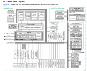
    SoC internal interconnect-wise, the R5FSS should be able to access PCIe based on below diagram.

    However, as a disclaimer that I will reiterate again, PCIe using RTOS (which also means PCIe through R5F MCU) has never been validated, and we do not have plans to enable this in the SDK either.

    Regards,

    Takuma

  • Hi Takuma,

    we got one step further.

    After I commented/removed the line

            setup_main_r5f_qos();

    (Line 567 in j721e_init.c which I pasted 2 posts earlier)

    MCU2_0 successfully read/writes PCIE2_DAT0.

    It turns out, that my "gut-feelings" about QoS have been correct to a certain degree.
    We searched in TRM of TDA4 and also in TRM of AM65 to get an idea what this specific QoS configuration means, and why it causes this kind of error. Without success.

    Can you please help us to understand what this specific QoS config from TI does, and why it prevents that mcu2_0 (and potential other cores) can't access PCIE2_DAT0?

    Maybe you can redirect me to a colleague of you, which has more experience in that part of TDA4 if necessary?

    Thank you and happy new year,

    Thomas

  • Hi Thomas,

    setup_main_r5f_qos sets up order ID (mainly used for parallel processing and load balancing), priority (mainly used for arbitration to give priority to certain threads), and lastly atype (which determines address type between not translated, intermediate, virtual, or translated physical). 

    The order ID and priority should not affect R5F view of PCIe, but I can believe atype would affect the view of memory. An atype of 0x0 and 0x3 are physical address types while 0x1 and 0x2 are routed to PVU/PAT+PVU or SMMU respectively for translation. I assume commenting out the R5F QoS setup makes atype into 0x0 to bypass any address translation.

    Regards,

    Takuma