AM6421: OSPI frame is split?

Part Number: AM6421
Other Parts Discussed in Thread: SYSCONFIG

Tool/software:

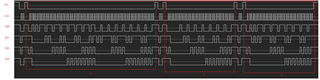
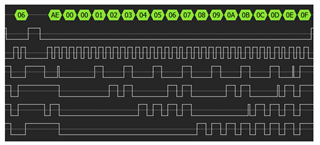
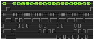
In direct mode, the clock is 10 M.

By calling the interface as shown in the figure above, the waveform is as follows.

A frame is split into three frames.

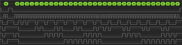
I want to know if this phenomenon is correct?

  • Hi Ryan,

    For NOR Flashes, OSPI Write direct is not possible/supported.

    The reasoning is mentioned here: https://e2e.ti.com/support/processors-group/processors/f/processors-forum/1448730/am6421-does-ospi-support-dma/5561444#5561444

    Regards,

    Vaibhav

  • Hi Vaibhav,

    I'm not operating NOR flash.

    The scenario is to use OSPI and FPGA for communication. 

    I just want to know if this kind of frame-splitting scene is as expected.

    BR

    Ryan

  • Hi Ryan,

    I'm not operating NOR flash.

    Okay I understood.

    The write operation happens in some chunks of memory sizes, so maybe that is why you are seeing frame splitting.

    Can you please attach a more clarifying diagram? I cannot understand what is clock/data lines/chip select line.

    Regards,

    Vaibhav

  • Hi Vaibhav,

    The write operation starts at address 0x00 with a quantity of 0x40.

    On the waveform, it is observed to be split into three frames, in sequence:

    The first frame starts at address 0x10 with a quantity of 0x20.

    The second frame starts at address 0x00 with a quantity of 0x10.

    The third frame starts at address 0x30 with a quantity of 0x10.

    Other observations,address 0x10 is written before 0x00.

    BR

    Ryan

  • Hi Ryan,

    with a quantity of 0x40

    What do you mean by quantity here?

    Regards,

    Vaibhav

  • Hi Vaibhav,

    When writing data, you need to have a starting address and size, which may be described here as a more appropriate size。

    BR

    Ryan

  • Hi Ryan,

    So just to confirm.

    The write operation starts at address 0x00 with a quantity of 0x40.

    This is like entire frame starting at address 0x0 and 64 bytes being transferred?

    The third frame starts at address 0x30 with a quantity of 0x10.

    And last frame starting at address 0x30 and sending 16 bytes of data?

    Can you tell me more about what this address here is?

    When you say that the entire frame starts at address 0x0, does this means that you are writing to the flash at offset 0x0?

    Please clarify my understandings.

    Regards,

    Vaibhav

  • Hi Vaibhav,

    Yes, address is mean that offset.

    BR

    Ryan

  • Hi Ryan,

    Yes, address is mean that offset.

    Okay I got it. 

    I will check the diagrams which you have attached, and I am assuming that you initiated the transfer write direct just once with address/flash offset as 0x0 and size as 64 bytes, but then you saw 3 frames being sent out instead of just one big frame consisting of 64 bytes.

    Moreover, is your SBL Null/Bootloader image flashed at offset 0x0 in the flash? If that is the case, it is recommended to not write any value to 0x0 offset as it will overwrite your SBL Null flashed image.

    Regards,

    Vaibhav

  • Hi Vaibhav,

    I will check the diagrams which you have attached, and I am assuming that you initiated the transfer write direct just once with address/flash offset as 0x0 and size as 64 bytes, but then you saw 3 frames being sent out instead of just one big frame consisting of 64 bytes.”,Yes, that's the case.

    Also, thank you for the reminder, this is another device on the bus operation, with a different CS, and the NOR flash will not respond.

    BR

    Ryan

  • Hi Kumar

    As offline discussed, here are several questions need to be clarified.

    1.  Is this expected behavior of our silicon that one transfer with 3 separated frame?

    2. Can this mechanism be turned off that split the frame? 

    Regards

    Zekun

  • Hi Ryan,

    Can you try using the top level API, in this case Flash_write(), because Flash_write() will call your write direct but maybe does some sort of initialization which you might be missing because you are calling the write direct API standalone.

    Can you please try it and let me know how it goes?

    Regards,

    Vaibhav

  • Hi Vaibhav,

    When I try to using the top level API, this situation will still exist.

    BR

    Ryan

  • Hi Vaibhav,

    When I try to using the top level API, this situation will still exist.

    BR

    Ryan

  • Hi Ryan,

    One way to confirm this for me would be to probe it, basically the lines, but it is hard to do so on the TI EVM.

    I will check if its possible to do so internally.

    1. Apart from this can you please remind me of the SDK version you are using so that I can go ahead and check the write Direct API implementation.
    2. Also please attach the datasheet or some relevant document I can go through to see the flash part being written to(could be FPGA).

    Regards,

    Vaibhav

  • Hi Ryan,

    I looked at the waveform you provided and was not sure if you captured the correct information for us.

    Data 0x06 is similar to the write enable command.

    I checked the OSPI flash from another vendor, and the timing is like this. How do we support OSPI NAND Flash if the OSPI NAND controller is not within specification? Thanks.


      Linjun

  • Hi,

    Apart from this can you please remind me of the SDK version you are using so that I can go ahead and check the write Direct API implementation.

    Since this has not been given out, I am checking the latest version and will provide an update in a day about the implementation of Flash_write() API.

    Regards,

    Vaibhav

  • Hi Vaibhav, we tested on AM64x MCU+ SDK 10.00.00 and 10.01.00.

  • Hi Linjun, there is no OSPI NAND Flash in ticket. We used OSPI communication between AM64x and FPGA.

  • The OSPI interface is used as the foundation for NAND/NOR memory and JEDEC specifications. It is a misconception to use it directly as an OSPI communication interface

  • Hi,

    I have a quick question.

    I am debugging inside the write API and you can expect responses in sometime.

    Meanwhile I am doing this, I am pretty sure you have implemented this, but if not can you check erase operation is happening before you start writing?

    I believe so that the memory space to be written to needs to be erased first.

    Regards,

    Vaibhav

  • Hi Vicent,

        Refer to the chapter 12.3.2.5.4, Interface support for working legacy mode, in spriuim2h.pdf. As for the limited depth of TX-FIFO and RX-FIFO, the registers OSPI_TX_THRESH_REG and OSPI_RX_THRESH_REG will be used, with a maximum size of 32 bytes. Dump both registers to check if the threshold is reasonable. If the transaction length is greater than the FIFO depth, the frames are split accordingly.

    Linjun

  • Hi,

    The internal SW implementation simply enables DAC for OSPI_readDirect and does a simple memcopy as per AM64x MCU PLUS SDK implementation from 10.0 and 10.1.

    The implementation of write direct on a MCU PLUS SDK for a different Sitara SoC like AM62A is a bit different. Please check the implementation and try the same.

    Regards,

    Vaibhav

  • Move the reply to this thread and close another one.

    Hi,

    The OSPI performance can be found here: https://software-dl.ti.com/mcu-plus-sdk/esd/AM64X/10_01_00_32/exports/docs/api_guide_am64x/DATASHEET_AM243X_EVM.html#autotoc_md491

    Moreover, can you also state the memory type of the FPGA which is used in communication? Is it NOR or NAND?

    Regards,

    Vaibhav

  • Hi Vaibhav,

      Below waveform is captured by customer to read Nor Flash (W25Q256JVFQ 128 byte. We can see the low level OSPI controller read these 128 bytes by two transactions, the first frame is form 0x0 to 0x53, the second transaction from 0x40 to 0x7F, 

       The issue is why overlap data transaction happened?  And there is no regular frame size, what's the low level OPSI controller behavior? Please response the issue directly or turn help the OSPI controller IP owner. Thanks.


    Regards,

    Linjun

  • Hi,

    Please response the issue directly or turn help the OSPI controller IP owner.

    I will include the relevant engineers.

    1. Apart from this, please confirm if to read the 128 bytes of data from the flash part, the customer used the OSPI_readDirect API?
    2. Also ask the customer to share the SysConfig file for the project so that I can quickly go ahead and review the flash configuration values they have put.

    Looking forward to your response.

    Regards,

    Vaibhav

  • Hi,

    1. The interface used is the OSPI_readDirect API.

    2. The configuration is as follows:

    /**
     * Write custom configuration values to the imported modules.
     */
    flash1.$name                           = "CONFIG_FLASH0";
    flash1.device                          = "CUSTOM_FLASH";
    flash1.skipHwInit                      = true;
    flash1.fname                           = "W25Q256";
    flash1.protocol                        = "1s_1s_4s";
    flash1.flashSize                       = 33554432;
    flash1.flashManfId                     = "0xEF";
    flash1.flashBlockSize                  = 65536;
    flash1.cmdBlockErase3B                 = "0xD8";
    flash1.cmdBlockErase4B                 = "0xD8";
    flash1.cmdSectorErase3B                = "0x20";
    flash1.cmdSectorErase4B                = "0x20";
    flash1.cmdRd                           = "0x6C";
    flash1.cmdWr                           = "0x32";
    flash1.dummyClksCmd                    = 0;
    flash1.dummyClksRd                     = 8;
    flash1.flashQeType                     = "4";
    flash1.proto_isAddrReg                 = false;
    flash1.dummy_isAddrReg                 = false;
    flash1.strDtr_isAddrReg                = false;
    flash1.resetType                       = "0x30";
    flash1.cmdExtType                      = "NONE";
    flash1.xspiWipRdCmd                    = "0x00";
    flash1.xspiWipReg                      = "0x00000000";
    flash1.idNumBytes                      = 5;
    flash1.dummyId8                        = 0;
    flash1.fourByteEnableSeq               = "0xA5";
    flash1.flashDeviceBusyTimeout          = 80000000;
    flash1.flashPageProgTimeout            = 704;
    flash1.flashDeviceId                   = "0x7019";
    flash1.peripheralDriver.$name          = "CONFIG_OSPI0";
    flash1.peripheralDriver.inputClkFreq   = 200000000;
    flash1.peripheralDriver.dmaEnable      = true;
    flash1.peripheralDriver.baudRateDiv    = 20;
    flash1.peripheralDriver.OSPI.CLK.rx    = true;
    flash1.peripheralDriver.OSPI.DQS.$used = false;
    flash1.peripheralDriver.OSPI.D7.rx     = false;
    flash1.peripheralDriver.OSPI.D7.$used  = false;
    flash1.peripheralDriver.OSPI.D6.rx     = false;
    flash1.peripheralDriver.OSPI.D6.$used  = false;
    flash1.peripheralDriver.OSPI.D5.rx     = false;
    flash1.peripheralDriver.OSPI.D5.$used  = false;
    flash1.peripheralDriver.OSPI.D4.rx     = false;
    flash1.peripheralDriver.OSPI.D4.$used  = false;

    BR

    Ryan

  • Hi,

    Your effective frequency is 200/20 = 10 MHz. I am sure if you have tested at different frequencies the behaviour of the read is the same.

    I am discussing this internally and would provide an update after a round of discussion.

    Regards,

    Vaibhav

  • Hi Ryan,

    When you send some bytes or receive some bytes then the frame splitting/overlapping is something to be looked for as this should not happen. 

    Reason:

    For write direct and read Direct API, the implementation at low level is just a simple memcopy operation, and based on your last response, a read for 128 bytes via memcopy should be one single transaction with no overlapping.

    I have increased the priority of this issue for wider visibility and will provide response on the same when we progress.

    Regards,

    Vaibhav

  • Hi Ryan,

         Could you please use attached script to dump OSPI registers and share to here?  Thanks.

         /cfs-file/__key/communityserver-discussions-components-files/791/1462.AM64_5F00_OSPI.tar.xz

    Linjun

  • Hi Linjun,

    Registers value as follows:

    CortexA53_0: GEL Output: OSPI0__OSPI_CFG_VBUSP__VBP2APB_WRAP__OSPI_CFG_VBP__OSPI_FLASH_APB_REGS_config_reg:Reg_0x0FC40000 : 0x80483841
    CortexA53_0: GEL Output: OSPI0__OSPI_CFG_VBUSP__VBP2APB_WRAP__OSPI_CFG_VBP__OSPI_FLASH_APB_REGS_dev_instr_rd_config_reg:Reg_0x0FC40004 : 0x0802006C
    CortexA53_0: GEL Output: OSPI0__OSPI_CFG_VBUSP__VBP2APB_WRAP__OSPI_CFG_VBP__OSPI_FLASH_APB_REGS_dev_instr_wr_config_reg:Reg_0x0FC40008 : 0x00020032
    CortexA53_0: GEL Output: OSPI0__OSPI_CFG_VBUSP__VBP2APB_WRAP__OSPI_CFG_VBP__OSPI_FLASH_APB_REGS_dev_delay_reg:Reg_0x0FC4000C : 0x0A0A0A0A
    CortexA53_0: GEL Output: OSPI0__OSPI_CFG_VBUSP__VBP2APB_WRAP__OSPI_CFG_VBP__OSPI_FLASH_APB_REGS_rd_data_capture_reg:Reg_0x0FC40010 : 0x00000029
    CortexA53_0: GEL Output: OSPI0__OSPI_CFG_VBUSP__VBP2APB_WRAP__OSPI_CFG_VBP__OSPI_FLASH_APB_REGS_dev_size_config_reg:Reg_0x0FC40014 : 0x00101003
    CortexA53_0: GEL Output: OSPI0__OSPI_CFG_VBUSP__VBP2APB_WRAP__OSPI_CFG_VBP__OSPI_FLASH_APB_REGS_sram_partition_cfg_reg:Reg_0x0FC40018 : 0x0000003F
    CortexA53_0: GEL Output: OSPI0__OSPI_CFG_VBUSP__VBP2APB_WRAP__OSPI_CFG_VBP__OSPI_FLASH_APB_REGS_ind_AHB_addr_trigger_reg:Reg_0x0FC4001C : 0x00000000
    CortexA53_0: GEL Output: OSPI0__OSPI_CFG_VBUSP__VBP2APB_WRAP__OSPI_CFG_VBP__OSPI_FLASH_APB_REGS_dma_periph_config_reg:Reg_0x0FC40020 : 0x00000000
    CortexA53_0: GEL Output: OSPI0__OSPI_CFG_VBUSP__VBP2APB_WRAP__OSPI_CFG_VBP__OSPI_FLASH_APB_REGS_remap_addr_reg:Reg_0x0FC40024 : 0x00000000
    CortexA53_0: GEL Output: OSPI0__OSPI_CFG_VBUSP__VBP2APB_WRAP__OSPI_CFG_VBP__OSPI_FLASH_APB_REGS_mode_bit_config_reg:Reg_0x0FC40028 : 0x00000000
    CortexA53_0: GEL Output: OSPI0__OSPI_CFG_VBUSP__VBP2APB_WRAP__OSPI_CFG_VBP__OSPI_FLASH_APB_REGS_sram_fill_reg:Reg_0x0FC4002C : 0x00000000
    CortexA53_0: GEL Output: OSPI0__OSPI_CFG_VBUSP__VBP2APB_WRAP__OSPI_CFG_VBP__OSPI_FLASH_APB_REGS_tx_thresh_reg:Reg_0x0FC40030 : 0x00000001
    CortexA53_0: GEL Output: OSPI0__OSPI_CFG_VBUSP__VBP2APB_WRAP__OSPI_CFG_VBP__OSPI_FLASH_APB_REGS_rx_thresh_reg:Reg_0x0FC40034 : 0x00000001
    CortexA53_0: GEL Output: OSPI0__OSPI_CFG_VBUSP__VBP2APB_WRAP__OSPI_CFG_VBP__OSPI_FLASH_APB_REGS_write_completion_ctrl_reg:Reg_0x0FC40038 : 0x000340FF
    CortexA53_0: GEL Output: OSPI0__OSPI_CFG_VBUSP__VBP2APB_WRAP__OSPI_CFG_VBP__OSPI_FLASH_APB_REGS_no_of_polls_bef_exp_reg:Reg_0x0FC4003C : 0xFFFFFFFF
    CortexA53_0: GEL Output: OSPI0__OSPI_CFG_VBUSP__VBP2APB_WRAP__OSPI_CFG_VBP__OSPI_FLASH_APB_REGS_irq_status_reg:Reg_0x0FC40040 : 0x00000000
    CortexA53_0: GEL Output: OSPI0__OSPI_CFG_VBUSP__VBP2APB_WRAP__OSPI_CFG_VBP__OSPI_FLASH_APB_REGS_irq_mask_reg:Reg_0x0FC40044 : 0x00000000
    CortexA53_0: GEL Output: OSPI0__OSPI_CFG_VBUSP__VBP2APB_WRAP__OSPI_CFG_VBP__OSPI_FLASH_APB_REGS_lower_wr_prot_reg:Reg_0x0FC40050 : 0x00000000
    CortexA53_0: GEL Output: OSPI0__OSPI_CFG_VBUSP__VBP2APB_WRAP__OSPI_CFG_VBP__OSPI_FLASH_APB_REGS_upper_wr_prot_reg:Reg_0x0FC40054 : 0x00000000
    CortexA53_0: GEL Output: OSPI0__OSPI_CFG_VBUSP__VBP2APB_WRAP__OSPI_CFG_VBP__OSPI_FLASH_APB_REGS_wr_prot_ctrl_reg:Reg_0x0FC40058 : 0x00000000
    CortexA53_0: GEL Output: OSPI0__OSPI_CFG_VBUSP__VBP2APB_WRAP__OSPI_CFG_VBP__OSPI_FLASH_APB_REGS_indirect_read_xfer_watermark_reg:Reg_0x0FC40064 : 0x00000000
    CortexA53_0: GEL Output: OSPI0__OSPI_CFG_VBUSP__VBP2APB_WRAP__OSPI_CFG_VBP__OSPI_FLASH_APB_REGS_indirect_read_xfer_start_reg:Reg_0x0FC40068 : 0x00000000
    CortexA53_0: GEL Output: OSPI0__OSPI_CFG_VBUSP__VBP2APB_WRAP__OSPI_CFG_VBP__OSPI_FLASH_APB_REGS_indirect_read_xfer_num_bytes_reg:Reg_0x0FC4006C : 0x00000000
    CortexA53_0: GEL Output: OSPI0__OSPI_CFG_VBUSP__VBP2APB_WRAP__OSPI_CFG_VBP__OSPI_FLASH_APB_REGS_indirect_write_xfer_watermark_reg:Reg_0x0FC40074 : 0xFFFFFFFF
    CortexA53_0: GEL Output: OSPI0__OSPI_CFG_VBUSP__VBP2APB_WRAP__OSPI_CFG_VBP__OSPI_FLASH_APB_REGS_indirect_write_xfer_start_reg:Reg_0x0FC40078 : 0x00000000
    CortexA53_0: GEL Output: OSPI0__OSPI_CFG_VBUSP__VBP2APB_WRAP__OSPI_CFG_VBP__OSPI_FLASH_APB_REGS_indirect_write_xfer_num_bytes_reg:Reg_0x0FC4007C : 0x00000000
    CortexA53_0: GEL Output: OSPI0__OSPI_CFG_VBUSP__VBP2APB_WRAP__OSPI_CFG_VBP__OSPI_FLASH_APB_REGS_indirect_trigger_addr_range_reg:Reg_0x0FC40080 : 0x00000004
    CortexA53_0: GEL Output: OSPI0__OSPI_CFG_VBUSP__VBP2APB_WRAP__OSPI_CFG_VBP__OSPI_FLASH_APB_REGS_flash_cmd_addr_reg:Reg_0x0FC40094 : 0x00800004
    CortexA53_0: GEL Output: OSPI0__OSPI_CFG_VBUSP__VBP2APB_WRAP__OSPI_CFG_VBP__OSPI_FLASH_APB_REGS_flash_rd_data_lower_reg:Reg_0x0FC400A0 : 0x00000021
    CortexA53_0: GEL Output: OSPI0__OSPI_CFG_VBUSP__VBP2APB_WRAP__OSPI_CFG_VBP__OSPI_FLASH_APB_REGS_flash_rd_data_upper_reg:Reg_0x0FC400A4 : 0x00000000
    CortexA53_0: GEL Output: OSPI0__OSPI_CFG_VBUSP__VBP2APB_WRAP__OSPI_CFG_VBP__OSPI_FLASH_APB_REGS_flash_wr_data_lower_reg:Reg_0x0FC400A8 : 0x00000020
    CortexA53_0: GEL Output: OSPI0__OSPI_CFG_VBUSP__VBP2APB_WRAP__OSPI_CFG_VBP__OSPI_FLASH_APB_REGS_flash_wr_data_upper_reg:Reg_0x0FC400AC : 0x00000000
    CortexA53_0: GEL Output: OSPI0__OSPI_CFG_VBUSP__VBP2APB_WRAP__OSPI_CFG_VBP__OSPI_FLASH_APB_REGS_polling_flash_status_reg:Reg_0x0FC400B0 : 0x00000000
    CortexA53_0: GEL Output: OSPI0__OSPI_CFG_VBUSP__VBP2APB_WRAP__OSPI_CFG_VBP__OSPI_FLASH_APB_REGS_phy_master_control_reg:Reg_0x0FC400B8 : 0x00800000
    CortexA53_0: GEL Output: OSPI0__OSPI_CFG_VBUSP__VBP2APB_WRAP__OSPI_CFG_VBP__OSPI_FLASH_APB_REGS_dll_observable_lower_reg:Reg_0x0FC400BC : 0x00FF81F9
    CortexA53_0: GEL Output: OSPI0__OSPI_CFG_VBUSP__VBP2APB_WRAP__OSPI_CFG_VBP__OSPI_FLASH_APB_REGS_dll_observable_upper_reg:Reg_0x0FC400C0 : 0x00000000
    CortexA53_0: GEL Output: OSPI0__OSPI_CFG_VBUSP__VBP2APB_WRAP__OSPI_CFG_VBP__OSPI_FLASH_APB_REGS_opcode_ext_lower_reg:Reg_0x0FC400E0 : 0x0302FA00
    CortexA53_0: GEL Output: OSPI0__OSPI_CFG_VBUSP__VBP2APB_WRAP__OSPI_CFG_VBP__OSPI_FLASH_APB_REGS_opcode_ext_upper_reg:Reg_0x0FC400E4 : 0x06F90000
    CortexA53_0: GEL Output: OSPI0__OSPI_CFG_VBUSP__VBP2APB_WRAP__OSPI_CFG_VBP__OSPI_FLASH_APB_REGS_module_id_reg:Reg_0x0FC400FC : 0x03000300
    CortexA53_0: GEL Output: OSPI0__OSPI_CFG_VBUSP__MMR__MMRVBP__REGS_PID:Reg_0x0FC44000 : 0x68747900
    CortexA53_0: GEL Output: OSPI0__OSPI_CFG_VBUSP__MMR__MMRVBP__REGS_CTRL:Reg_0x0FC44004 : 0x00000000
    CortexA53_0: GEL Output: OSPI0__OSPI_CFG_VBUSP__MMR__MMRVBP__REGS_STAT:Reg_0x0FC44008 : 0x00000002

    BR

    Ryan

  • Hello Ryan,

    Question for you:

    The flash configuration values are incorrectly configured.

    You have mentioned few values here: https://e2e.ti.com/support/processors-group/processors/f/processors-forum/1450567/am6421-ospi-frame-is-split/5653718#5653718

    I have checked the datasheet and turns out that the following values are incorrect for which I have written the comments in red

    Action item on me:

    Within sometime, I will probe the data lines and check for the overlapping behaviour which is unexpected.

    Regards,
    Vaibhav

  • Hello experts,

    To focus on the objective, here is the summary.

    Issue we met:

    • Each reading or writing was divided into several requests
    • Don't know how many requests divided for different data length of reading and writing
    • Uncertain behavior
    • Lower performance of reading and writing vs OSPI reading/writing operation.​

    Supports we need:

    • Need OSPI communication to read/write operation
      • Each reading operation should have one request sending to device
      • Each writing operation should have one request sending to device
    • Need a solution to avoid divided into several requests for each OSPI reading/writing operation.

    Let me  know if you have any question.

  • Hi Ryan,

    The following are some recommendations for optimizing transaction behavior based on register dump results.

    1 Use indirect mode to access the ospi controller

    2 With STIG enabled, we can set the number of bytes read by the STIG memory library in the current case.

    3 Refresh the OSPI controller pipe by setting FSS0_OSPI0_SS_CFG bit 3 to 1 before read and write operations.

    Please feedback  the result. Thanks.

    Linjun

  • Hi Linjun,

    1.  The read operation in the indirect mode is split into multiple requests.

    2.  Registers value as follows:

    CortexA53_0: GEL Output: OSPI0__OSPI_CFG_VBUSP__VBP2APB_WRAP__OSPI_CFG_VBP__OSPI_FLASH_APB_REGS_config_reg:Reg_0x0FC40000 : 0x80083841
    CortexA53_0: GEL Output: OSPI0__OSPI_CFG_VBUSP__VBP2APB_WRAP__OSPI_CFG_VBP__OSPI_FLASH_APB_REGS_dev_instr_rd_config_reg:Reg_0x0FC40004 : 0x0802006C
    CortexA53_0: GEL Output: OSPI0__OSPI_CFG_VBUSP__VBP2APB_WRAP__OSPI_CFG_VBP__OSPI_FLASH_APB_REGS_dev_instr_wr_config_reg:Reg_0x0FC40008 : 0x00020032
    CortexA53_0: GEL Output: OSPI0__OSPI_CFG_VBUSP__VBP2APB_WRAP__OSPI_CFG_VBP__OSPI_FLASH_APB_REGS_dev_delay_reg:Reg_0x0FC4000C : 0x0A0A0A0A
    CortexA53_0: GEL Output: OSPI0__OSPI_CFG_VBUSP__VBP2APB_WRAP__OSPI_CFG_VBP__OSPI_FLASH_APB_REGS_rd_data_capture_reg:Reg_0x0FC40010 : 0x00000029
    CortexA53_0: GEL Output: OSPI0__OSPI_CFG_VBUSP__VBP2APB_WRAP__OSPI_CFG_VBP__OSPI_FLASH_APB_REGS_dev_size_config_reg:Reg_0x0FC40014 : 0x00101003
    CortexA53_0: GEL Output: OSPI0__OSPI_CFG_VBUSP__VBP2APB_WRAP__OSPI_CFG_VBP__OSPI_FLASH_APB_REGS_sram_partition_cfg_reg:Reg_0x0FC40018 : 0x0000003F
    CortexA53_0: GEL Output: OSPI0__OSPI_CFG_VBUSP__VBP2APB_WRAP__OSPI_CFG_VBP__OSPI_FLASH_APB_REGS_ind_AHB_addr_trigger_reg:Reg_0x0FC4001C : 0x00000000
    CortexA53_0: GEL Output: OSPI0__OSPI_CFG_VBUSP__VBP2APB_WRAP__OSPI_CFG_VBP__OSPI_FLASH_APB_REGS_dma_periph_config_reg:Reg_0x0FC40020 : 0x00000000
    CortexA53_0: GEL Output: OSPI0__OSPI_CFG_VBUSP__VBP2APB_WRAP__OSPI_CFG_VBP__OSPI_FLASH_APB_REGS_remap_addr_reg:Reg_0x0FC40024 : 0x00000000
    CortexA53_0: GEL Output: OSPI0__OSPI_CFG_VBUSP__VBP2APB_WRAP__OSPI_CFG_VBP__OSPI_FLASH_APB_REGS_mode_bit_config_reg:Reg_0x0FC40028 : 0x00000000
    CortexA53_0: GEL Output: OSPI0__OSPI_CFG_VBUSP__VBP2APB_WRAP__OSPI_CFG_VBP__OSPI_FLASH_APB_REGS_sram_fill_reg:Reg_0x0FC4002C : 0x00000000
    CortexA53_0: GEL Output: OSPI0__OSPI_CFG_VBUSP__VBP2APB_WRAP__OSPI_CFG_VBP__OSPI_FLASH_APB_REGS_tx_thresh_reg:Reg_0x0FC40030 : 0x00000001
    CortexA53_0: GEL Output: OSPI0__OSPI_CFG_VBUSP__VBP2APB_WRAP__OSPI_CFG_VBP__OSPI_FLASH_APB_REGS_rx_thresh_reg:Reg_0x0FC40034 : 0x00000001
    CortexA53_0: GEL Output: OSPI0__OSPI_CFG_VBUSP__VBP2APB_WRAP__OSPI_CFG_VBP__OSPI_FLASH_APB_REGS_write_completion_ctrl_reg:Reg_0x0FC40038 : 0x000340FF
    CortexA53_0: GEL Output: OSPI0__OSPI_CFG_VBUSP__VBP2APB_WRAP__OSPI_CFG_VBP__OSPI_FLASH_APB_REGS_no_of_polls_bef_exp_reg:Reg_0x0FC4003C : 0xFFFFFFFF
    CortexA53_0: GEL Output: OSPI0__OSPI_CFG_VBUSP__VBP2APB_WRAP__OSPI_CFG_VBP__OSPI_FLASH_APB_REGS_irq_status_reg:Reg_0x0FC40040 : 0x00000000
    CortexA53_0: GEL Output: OSPI0__OSPI_CFG_VBUSP__VBP2APB_WRAP__OSPI_CFG_VBP__OSPI_FLASH_APB_REGS_irq_mask_reg:Reg_0x0FC40044 : 0x00000000
    CortexA53_0: GEL Output: OSPI0__OSPI_CFG_VBUSP__VBP2APB_WRAP__OSPI_CFG_VBP__OSPI_FLASH_APB_REGS_lower_wr_prot_reg:Reg_0x0FC40050 : 0x00000000
    CortexA53_0: GEL Output: OSPI0__OSPI_CFG_VBUSP__VBP2APB_WRAP__OSPI_CFG_VBP__OSPI_FLASH_APB_REGS_upper_wr_prot_reg:Reg_0x0FC40054 : 0x00000000
    CortexA53_0: GEL Output: OSPI0__OSPI_CFG_VBUSP__VBP2APB_WRAP__OSPI_CFG_VBP__OSPI_FLASH_APB_REGS_wr_prot_ctrl_reg:Reg_0x0FC40058 : 0x00000000
    CortexA53_0: GEL Output: OSPI0__OSPI_CFG_VBUSP__VBP2APB_WRAP__OSPI_CFG_VBP__OSPI_FLASH_APB_REGS_indirect_read_xfer_watermark_reg:Reg_0x0FC40064 : 0x00000010
    CortexA53_0: GEL Output: OSPI0__OSPI_CFG_VBUSP__VBP2APB_WRAP__OSPI_CFG_VBP__OSPI_FLASH_APB_REGS_indirect_read_xfer_start_reg:Reg_0x0FC40068 : 0x01000000
    CortexA53_0: GEL Output: OSPI0__OSPI_CFG_VBUSP__VBP2APB_WRAP__OSPI_CFG_VBP__OSPI_FLASH_APB_REGS_indirect_read_xfer_num_bytes_reg:Reg_0x0FC4006C : 0x00000080
    CortexA53_0: GEL Output: OSPI0__OSPI_CFG_VBUSP__VBP2APB_WRAP__OSPI_CFG_VBP__OSPI_FLASH_APB_REGS_indirect_write_xfer_watermark_reg:Reg_0x0FC40074 : 0xFFFFFFFF
    CortexA53_0: GEL Output: OSPI0__OSPI_CFG_VBUSP__VBP2APB_WRAP__OSPI_CFG_VBP__OSPI_FLASH_APB_REGS_indirect_write_xfer_start_reg:Reg_0x0FC40078 : 0x00000000
    CortexA53_0: GEL Output: OSPI0__OSPI_CFG_VBUSP__VBP2APB_WRAP__OSPI_CFG_VBP__OSPI_FLASH_APB_REGS_indirect_write_xfer_num_bytes_reg:Reg_0x0FC4007C : 0x00000000
    CortexA53_0: GEL Output: OSPI0__OSPI_CFG_VBUSP__VBP2APB_WRAP__OSPI_CFG_VBP__OSPI_FLASH_APB_REGS_indirect_trigger_addr_range_reg:Reg_0x0FC40080 : 0x00000004
    CortexA53_0: GEL Output: OSPI0__OSPI_CFG_VBUSP__VBP2APB_WRAP__OSPI_CFG_VBP__OSPI_FLASH_APB_REGS_flash_cmd_addr_reg:Reg_0x0FC40094 : 0x00800004
    CortexA53_0: GEL Output: OSPI0__OSPI_CFG_VBUSP__VBP2APB_WRAP__OSPI_CFG_VBP__OSPI_FLASH_APB_REGS_flash_rd_data_lower_reg:Reg_0x0FC400A0 : 0x00000021
    CortexA53_0: GEL Output: OSPI0__OSPI_CFG_VBUSP__VBP2APB_WRAP__OSPI_CFG_VBP__OSPI_FLASH_APB_REGS_flash_rd_data_upper_reg:Reg_0x0FC400A4 : 0x00000000
    CortexA53_0: GEL Output: OSPI0__OSPI_CFG_VBUSP__VBP2APB_WRAP__OSPI_CFG_VBP__OSPI_FLASH_APB_REGS_flash_wr_data_lower_reg:Reg_0x0FC400A8 : 0x00000020
    CortexA53_0: GEL Output: OSPI0__OSPI_CFG_VBUSP__VBP2APB_WRAP__OSPI_CFG_VBP__OSPI_FLASH_APB_REGS_flash_wr_data_upper_reg:Reg_0x0FC400AC : 0x00000000
    CortexA53_0: GEL Output: OSPI0__OSPI_CFG_VBUSP__VBP2APB_WRAP__OSPI_CFG_VBP__OSPI_FLASH_APB_REGS_polling_flash_status_reg:Reg_0x0FC400B0 : 0x00000000
    CortexA53_0: GEL Output: OSPI0__OSPI_CFG_VBUSP__VBP2APB_WRAP__OSPI_CFG_VBP__OSPI_FLASH_APB_REGS_phy_master_control_reg:Reg_0x0FC400B8 : 0x00800000
    CortexA53_0: GEL Output: OSPI0__OSPI_CFG_VBUSP__VBP2APB_WRAP__OSPI_CFG_VBP__OSPI_FLASH_APB_REGS_dll_observable_lower_reg:Reg_0x0FC400BC : 0x00FF81F9
    CortexA53_0: GEL Output: OSPI0__OSPI_CFG_VBUSP__VBP2APB_WRAP__OSPI_CFG_VBP__OSPI_FLASH_APB_REGS_dll_observable_upper_reg:Reg_0x0FC400C0 : 0x00000000
    CortexA53_0: GEL Output: OSPI0__OSPI_CFG_VBUSP__VBP2APB_WRAP__OSPI_CFG_VBP__OSPI_FLASH_APB_REGS_opcode_ext_lower_reg:Reg_0x0FC400E0 : 0x0302FA00
    CortexA53_0: GEL Output: OSPI0__OSPI_CFG_VBUSP__VBP2APB_WRAP__OSPI_CFG_VBP__OSPI_FLASH_APB_REGS_opcode_ext_upper_reg:Reg_0x0FC400E4 : 0x06F90000
    CortexA53_0: GEL Output: OSPI0__OSPI_CFG_VBUSP__VBP2APB_WRAP__OSPI_CFG_VBP__OSPI_FLASH_APB_REGS_module_id_reg:Reg_0x0FC400FC : 0x03000300
    CortexA53_0: GEL Output: OSPI0__OSPI_CFG_VBUSP__MMR__MMRVBP__REGS_PID:Reg_0x0FC44000 : 0x68747900
    CortexA53_0: GEL Output: OSPI0__OSPI_CFG_VBUSP__MMR__MMRVBP__REGS_CTRL:Reg_0x0FC44004 : 0x00000000
    CortexA53_0: GEL Output: OSPI0__OSPI_CFG_VBUSP__MMR__MMRVBP__REGS_STAT:Reg_0x0FC44008 : 0x00000002

    BR

    Ryan

  • Greetings Ryan,

    1. What exactly does this mean? Do you mean on the scope the indirect read?

    2. This register dump is missing a critical register, the Indirect Read Transfer Control Register at offset 0x0FC40060. This has a number of status bits relating to the transfer.

    Sincerely,

    Lucas

  • Ryan,

       I updated the gel to dump all the OSPI controller register as last  link. Please help dump accordingly. Thanks.

    Linjun

  • Hi Linjun,

    Registers value as follows:

    CortexA53_0: GEL Output: OSPI0__OSPI_CFG_VBUSP__VBP2APB_WRAP__OSPI_CFG_VBP__OSPI_FLASH_APB_REGS_config_reg:Reg_0x0FC40000 : 0x80483841
    CortexA53_0: GEL Output: OSPI0__OSPI_CFG_VBUSP__VBP2APB_WRAP__OSPI_CFG_VBP__OSPI_FLASH_APB_REGS_dev_instr_rd_config_reg:Reg_0x0FC40004 : 0x0802006C
    CortexA53_0: GEL Output: OSPI0__OSPI_CFG_VBUSP__VBP2APB_WRAP__OSPI_CFG_VBP__OSPI_FLASH_APB_REGS_dev_instr_wr_config_reg:Reg_0x0FC40008 : 0x00020032
    CortexA53_0: GEL Output: OSPI0__OSPI_CFG_VBUSP__VBP2APB_WRAP__OSPI_CFG_VBP__OSPI_FLASH_APB_REGS_dev_delay_reg:Reg_0x0FC4000C : 0x0A0A0A0A
    CortexA53_0: GEL Output: OSPI0__OSPI_CFG_VBUSP__VBP2APB_WRAP__OSPI_CFG_VBP__OSPI_FLASH_APB_REGS_rd_data_capture_reg:Reg_0x0FC40010 : 0x00000027
    CortexA53_0: GEL Output: OSPI0__OSPI_CFG_VBUSP__VBP2APB_WRAP__OSPI_CFG_VBP__OSPI_FLASH_APB_REGS_dev_size_config_reg:Reg_0x0FC40014 : 0x00101003
    CortexA53_0: GEL Output: OSPI0__OSPI_CFG_VBUSP__VBP2APB_WRAP__OSPI_CFG_VBP__OSPI_FLASH_APB_REGS_sram_partition_cfg_reg:Reg_0x0FC40018 : 0x0000003F
    CortexA53_0: GEL Output: OSPI0__OSPI_CFG_VBUSP__VBP2APB_WRAP__OSPI_CFG_VBP__OSPI_FLASH_APB_REGS_ind_AHB_addr_trigger_reg:Reg_0x0FC4001C : 0x00000000
    CortexA53_0: GEL Output: OSPI0__OSPI_CFG_VBUSP__VBP2APB_WRAP__OSPI_CFG_VBP__OSPI_FLASH_APB_REGS_dma_periph_config_reg:Reg_0x0FC40020 : 0x00000000
    CortexA53_0: GEL Output: OSPI0__OSPI_CFG_VBUSP__VBP2APB_WRAP__OSPI_CFG_VBP__OSPI_FLASH_APB_REGS_remap_addr_reg:Reg_0x0FC40024 : 0x00000000
    CortexA53_0: GEL Output: OSPI0__OSPI_CFG_VBUSP__VBP2APB_WRAP__OSPI_CFG_VBP__OSPI_FLASH_APB_REGS_mode_bit_config_reg:Reg_0x0FC40028 : 0x00000000
    CortexA53_0: GEL Output: OSPI0__OSPI_CFG_VBUSP__VBP2APB_WRAP__OSPI_CFG_VBP__OSPI_FLASH_APB_REGS_sram_fill_reg:Reg_0x0FC4002C : 0x00000000
    CortexA53_0: GEL Output: OSPI0__OSPI_CFG_VBUSP__VBP2APB_WRAP__OSPI_CFG_VBP__OSPI_FLASH_APB_REGS_tx_thresh_reg:Reg_0x0FC40030 : 0x00000001
    CortexA53_0: GEL Output: OSPI0__OSPI_CFG_VBUSP__VBP2APB_WRAP__OSPI_CFG_VBP__OSPI_FLASH_APB_REGS_rx_thresh_reg:Reg_0x0FC40034 : 0x00000001
    CortexA53_0: GEL Output: OSPI0__OSPI_CFG_VBUSP__VBP2APB_WRAP__OSPI_CFG_VBP__OSPI_FLASH_APB_REGS_write_completion_ctrl_reg:Reg_0x0FC40038 : 0x000340FF
    CortexA53_0: GEL Output: OSPI0__OSPI_CFG_VBUSP__VBP2APB_WRAP__OSPI_CFG_VBP__OSPI_FLASH_APB_REGS_no_of_polls_bef_exp_reg:Reg_0x0FC4003C : 0xFFFFFFFF
    CortexA53_0: GEL Output: OSPI0__OSPI_CFG_VBUSP__VBP2APB_WRAP__OSPI_CFG_VBP__OSPI_FLASH_APB_REGS_irq_status_reg:Reg_0x0FC40040 : 0x00000000
    CortexA53_0: GEL Output: OSPI0__OSPI_CFG_VBUSP__VBP2APB_WRAP__OSPI_CFG_VBP__OSPI_FLASH_APB_REGS_irq_mask_reg:Reg_0x0FC40044 : 0x00000000
    CortexA53_0: GEL Output: OSPI0__OSPI_CFG_VBUSP__VBP2APB_WRAP__OSPI_CFG_VBP__OSPI_FLASH_APB_REGS_lower_wr_prot_reg:Reg_0x0FC40050 : 0x00000000
    CortexA53_0: GEL Output: OSPI0__OSPI_CFG_VBUSP__VBP2APB_WRAP__OSPI_CFG_VBP__OSPI_FLASH_APB_REGS_upper_wr_prot_reg:Reg_0x0FC40054 : 0x00000000
    CortexA53_0: GEL Output: OSPI0__OSPI_CFG_VBUSP__VBP2APB_WRAP__OSPI_CFG_VBP__OSPI_FLASH_APB_REGS_wr_prot_ctrl_reg:Reg_0x0FC40058 : 0x00000000
    CortexA53_0: GEL Output: OSPI0__OSPI_CFG_VBUSP__VBP2APB_WRAP__OSPI_CFG_VBP__OSPI_FLASH_APB_REGS_indirect_read_xfer_ctrl_reg:Reg_0x0FC40060 : 0x00000000
    CortexA53_0: GEL Output: OSPI0__OSPI_CFG_VBUSP__VBP2APB_WRAP__OSPI_CFG_VBP__OSPI_FLASH_APB_REGS_indirect_read_xfer_watermark_reg:Reg_0x0FC40064 : 0x00000000
    CortexA53_0: GEL Output: OSPI0__OSPI_CFG_VBUSP__VBP2APB_WRAP__OSPI_CFG_VBP__OSPI_FLASH_APB_REGS_indirect_read_xfer_start_reg:Reg_0x0FC40068 : 0x00000000
    CortexA53_0: GEL Output: OSPI0__OSPI_CFG_VBUSP__VBP2APB_WRAP__OSPI_CFG_VBP__OSPI_FLASH_APB_REGS_indirect_read_xfer_num_bytes_reg:Reg_0x0FC4006C : 0x00000000
    CortexA53_0: GEL Output: OSPI0__OSPI_CFG_VBUSP__VBP2APB_WRAP__OSPI_CFG_VBP__OSPI_FLASH_APB_REGS_indirect_write_xfer_ctrl_reg:Reg_0x0FC40070 : 0x00000000
    CortexA53_0: GEL Output: OSPI0__OSPI_CFG_VBUSP__VBP2APB_WRAP__OSPI_CFG_VBP__OSPI_FLASH_APB_REGS_indirect_write_xfer_watermark_reg:Reg_0x0FC40074 : 0xFFFFFFFF
    CortexA53_0: GEL Output: OSPI0__OSPI_CFG_VBUSP__VBP2APB_WRAP__OSPI_CFG_VBP__OSPI_FLASH_APB_REGS_indirect_write_xfer_start_reg:Reg_0x0FC40078 : 0x00000000
    CortexA53_0: GEL Output: OSPI0__OSPI_CFG_VBUSP__VBP2APB_WRAP__OSPI_CFG_VBP__OSPI_FLASH_APB_REGS_indirect_write_xfer_num_bytes_reg:Reg_0x0FC4007C : 0x00000000
    CortexA53_0: GEL Output: OSPI0__OSPI_CFG_VBUSP__VBP2APB_WRAP__OSPI_CFG_VBP__OSPI_FLASH_APB_REGS_indirect_trigger_addr_range_reg:Reg_0x0FC40080 : 0x00000004
    CortexA53_0: GEL Output: OSPI0__OSPI_CFG_VBUSP__VBP2APB_WRAP__OSPI_CFG_VBP__OSPI_FLASH_APB_REGS_flash_command_ctrl_mem_reg:Reg_0x0FC4008C : 0x00000000
    CortexA53_0: GEL Output: OSPI0__OSPI_CFG_VBUSP__VBP2APB_WRAP__OSPI_CFG_VBP__OSPI_FLASH_APB_REGS_flash_cmd_ctrl_reg:Reg_0x0FC40090 : 0x11008000
    CortexA53_0: GEL Output: OSPI0__OSPI_CFG_VBUSP__VBP2APB_WRAP__OSPI_CFG_VBP__OSPI_FLASH_APB_REGS_flash_cmd_addr_reg:Reg_0x0FC40094 : 0x00800004
    CortexA53_0: GEL Output: OSPI0__OSPI_CFG_VBUSP__VBP2APB_WRAP__OSPI_CFG_VBP__OSPI_FLASH_APB_REGS_flash_rd_data_lower_reg:Reg_0x0FC400A0 : 0x00000021
    CortexA53_0: GEL Output: OSPI0__OSPI_CFG_VBUSP__VBP2APB_WRAP__OSPI_CFG_VBP__OSPI_FLASH_APB_REGS_flash_rd_data_upper_reg:Reg_0x0FC400A4 : 0x00000000
    CortexA53_0: GEL Output: OSPI0__OSPI_CFG_VBUSP__VBP2APB_WRAP__OSPI_CFG_VBP__OSPI_FLASH_APB_REGS_flash_wr_data_lower_reg:Reg_0x0FC400A8 : 0x00000020
    CortexA53_0: GEL Output: OSPI0__OSPI_CFG_VBUSP__VBP2APB_WRAP__OSPI_CFG_VBP__OSPI_FLASH_APB_REGS_flash_wr_data_upper_reg:Reg_0x0FC400AC : 0x00000000
    CortexA53_0: GEL Output: OSPI0__OSPI_CFG_VBUSP__VBP2APB_WRAP__OSPI_CFG_VBP__OSPI_FLASH_APB_REGS_polling_flash_status_reg:Reg_0x0FC400B0 : 0x00000000
    CortexA53_0: GEL Output: OSPI0__OSPI_CFG_VBUSP__VBP2APB_WRAP__OSPI_CFG_VBP__OSPI_FLASH_APB_REGS_phy_configuration_reg:Reg_0x0FC400B4 : 0x00000000
    CortexA53_0: GEL Output: OSPI0__OSPI_CFG_VBUSP__VBP2APB_WRAP__OSPI_CFG_VBP__OSPI_FLASH_APB_REGS_phy_master_control_reg:Reg_0x0FC400B8 : 0x00800000
    CortexA53_0: GEL Output: OSPI0__OSPI_CFG_VBUSP__VBP2APB_WRAP__OSPI_CFG_VBP__OSPI_FLASH_APB_REGS_dll_observable_lower_reg:Reg_0x0FC400BC : 0x00000000
    CortexA53_0: GEL Output: OSPI0__OSPI_CFG_VBUSP__VBP2APB_WRAP__OSPI_CFG_VBP__OSPI_FLASH_APB_REGS_dll_observable_upper_reg:Reg_0x0FC400C0 : 0x00000000
    CortexA53_0: GEL Output: OSPI0__OSPI_CFG_VBUSP__VBP2APB_WRAP__OSPI_CFG_VBP__OSPI_FLASH_APB_REGS_opcode_ext_lower_reg:Reg_0x0FC400E0 : 0x0302FA00
    CortexA53_0: GEL Output: OSPI0__OSPI_CFG_VBUSP__VBP2APB_WRAP__OSPI_CFG_VBP__OSPI_FLASH_APB_REGS_opcode_ext_upper_reg:Reg_0x0FC400E4 : 0x06F90000
    CortexA53_0: GEL Output: OSPI0__OSPI_CFG_VBUSP__VBP2APB_WRAP__OSPI_CFG_VBP__OSPI_FLASH_APB_REGS_module_id_reg:Reg_0x0FC400FC : 0x03000300
    CortexA53_0: GEL Output: OSPI0__OSPI_CFG_VBUSP__MMR__MMRVBP__REGS_PID:Reg_0x0FC44000 : 0x68747900
    CortexA53_0: GEL Output: OSPI0__OSPI_CFG_VBUSP__MMR__MMRVBP__REGS_CTRL:Reg_0x0FC44004 : 0x00000000
    CortexA53_0: GEL Output: OSPI0__OSPI_CFG_VBUSP__MMR__MMRVBP__REGS_STAT:Reg_0x0FC44008 : 0x00000002
    BR

    Ryan

  • Hi Ryan,

    Could you please fix this small bug in the MCU PLUS SDK 10.01 for AM64x?

    Inside ospi_lld.h, on line 182, can you go ahead and switch the position of data and addr?

    So the definition should look like as follows:

    Once done, please rebuild the libraries.

    And give your code a run.

    Why this change is happening?

    The function definition should be cmd, addr, data which follows 1s-1s-4s and it sets correctly.

    But, earlier in the SDK, it is written as cmd, data, addr which will make the setting as 1s-4s-1s, instead of desired 1s-1s-4s.

    Regards,

    Vaibhav

  • Hi Ryan,

    I am probing the lines to check the behaviour and I will update you best by starting of the next week as I am yet to get the clock line soldered.

    Post this I will see the behaviour and let you know.

    Regards,
    Vaibhav

  • Greetings Ryan,

    • One thing came up in discussion to double check, are the MPU region settings modified in any way from stock? Can you share the MPU configuration being done?
    • Regarding the register dumps, I see the registers but the latest dump all the indirect read registers look to be empty compared to the first one. Was this taken before or after the indirect read was triggered? The first one I assumed to be taken after the indirect read, but I think some clarification is needed on both of them.

    Sincerely,

    Lucas

  • Hi Vaibhav, 

    Thank you for your support.

    I look forward to hearing good news from you.

    BR

    Ryan

  • Hi Ryan

    • One thing came up in discussion to double check, are the MPU region settings modified in any way from stock? Can you share the MPU configuration being done?
    • Regarding the register dumps, I see the registers but the latest dump all the indirect read registers look to be empty compared to the first one. Was this taken before or after the indirect read was triggered? The first one I assumed to be taken after the indirect read, but I think some clarification is needed on both of them.

    Can you please respond to the questions from Lucas?

    1.  The read operation in the indirect mode is split into multiple requests.

    Do you have a scope capture for this? Or explain what was the split / overlap?

    Also,

    Regards

    Karan

  • Hi Lucas,

    1. We are using OSPI on the A53, so there is no MPU configuration, only MMU settings.

    2. The MMU configuration is as follows:

    MmuP_RegionConfig gMmuRegionConfig[CONFIG_MMU_NUM_REGIONS] =
    {
        {
            .vaddr = 0x0u,
            .paddr = 0x0u,
            .size = 0x80000000u,
            .attr = {
                .accessPerm = MMUP_ACCESS_PERM_PRIV_RW_USER_NONE,
                .privExecute = 1,
                .userExecute = 0,
                .shareable = MMUP_SHARABLE_OUTER,
                .attrIndx = MMUP_ATTRINDX_MAIR0,
                .global = 1
            }
        },
        {
            .vaddr = 0x70000000u,
            .paddr = 0x70000000u,
            .size = 0x200000u,
            .attr = {
                .accessPerm = MMUP_ACCESS_PERM_PRIV_RW_USER_NONE,
                .privExecute = 1,
                .userExecute = 0,
                .shareable = MMUP_SHARABLE_OUTER,
                .attrIndx = MMUP_ATTRINDX_MAIR7,
                .global = 1
            }
        },
        {
            .vaddr = 0x80000000u,
            .paddr = 0x80000000u,
            .size = 0x80000000u,
            .attr = {
                .accessPerm = MMUP_ACCESS_PERM_PRIV_RW_USER_NONE,
                .privExecute = 1,
                .userExecute = 0,
                .shareable = MMUP_SHARABLE_OUTER,
                .attrIndx = MMUP_ATTRINDX_MAIR7,
                .global = 1
            }
        },
        {
            .vaddr = 0x78100000u,
            .paddr = 0x78100000u,
            .size = 0x1000u,
            .attr = {
                .accessPerm = MMUP_ACCESS_PERM_PRIV_RW_USER_NONE,
                .privExecute = 0,
                .userExecute = 0,
                .shareable = MMUP_SHARABLE_OUTER,
                .attrIndx = MMUP_ATTRINDX_MAIR7,
                .global = 1
            }
        },
        {
            .vaddr = 0x701D0000u,
            .paddr = 0x701D0000u,
            .size = 0x10000u,
            .attr = {
                .accessPerm = MMUP_ACCESS_PERM_PRIV_RW_USER_NONE,
                .privExecute = 1,
                .userExecute = 0,
                .shareable = MMUP_SHARABLE_OUTER,
                .attrIndx = MMUP_ATTRINDX_MAIR4,
                .global = 1
            }
        },
    };

    3. The issue persists even when the memory that was attempted to be accessed is set to non-cacheable.

    4. Regarding the register dumps, I have not used any interfaces outside of the TI SDK, nor have I manually modified any interfaces or registers. Since I have not delved into such detailed aspects, I am unable to answer this question.

    BR

    Ryan

  • Hi Karan,

    About the "Do you have a scope capture for this? Or explain what was the split / overlap?", in the preceding text, Linjun has provided a detailed summary.

    BR

    Ryan

  • Hi Ryan,

        Here is a sampel code to send data to ospi interface, could you please check and feedback? obbisouly , the transmit lenght and memory attribute is desgined. Thanks.

    #define APP_OSPI_DATA_SIZE (2048)
    uint8_t gOspiTxBuf[APP_OSPI_DATA_SIZE];
    /* read buffer MUST be cache line aligned when using DMA, we aligned to 128B though 32B is enough */
    uint8_t gOspiRxBuf[APP_OSPI_DATA_SIZE] __attribute__((aligned(128U)));

     Linjun

  • Hi Linjun,

    The issue still persists even when the memory attribute is set to cache alignment.

    BR

    Ryan

  • Hi Ryan,

    Post our call today, I am supposed to send you waveforms for the following:

    1. 1s-1s-1s INDAC 128 bytes read from QSPI NOR Flash part. (Clock: 100 MHz, Clock Divider: 4)
       
      indirect_read_128bytes_1s_1s_1s.sal


    2. 4s-4d-4d INDAC 128 bytes read from QSPI NOR Flash part(For this we applied a glitch filter of 4 ns which is 10% of clock period)(Clock: 100 MHz, Clock Divider: 4)

      indirect_read_128bytes_4s_4d_4d.sal
    3. 8d-8d-8d INDAC 128 bytes read from OSPI NOR Flash Part(I got the soldering done for the TI EVM having OSPI NOR Flash, earlier for the above two captured waveforms the soldering was done on TI EVM having QSPI NOR Flash)[NOTE: I will be sending the waveform for this in sometime]

    The waveform as seen in both of these transactions, happens in 1 Chip Select low.

    How to view the waveform?

    To view the waveform simply head over to this website and download the Logic 2 software: https://www.saleae.com/pages/downloads

    Once downloaded, you can save the attached waveforms which have an extension of .sal and then simply click on it. It will automatically open the Logic 2 software and show the waveform.

    Regards,
    Vaibhav

  • Detailed steps on how to enable INDAC reads in the software:

    1. Go to the following file: C:\ti\mcu_plus_sdk_am64x_10_00_00_20\source\board\flash\ospi\flash_nor_ospi.c
    2. Inside the API Flash_norOspiRead, please change the OSPI_readDirect API call to OSPI_readIndirect
    3. Save the file and in a terminal please go the directory as shown in the screenshot and execute two commands:

    Once done, please go ahead and rebuild your application, this will make sure that the changes are taken into account.

    There you go, you have successfully enabled INDAC reads.

    Best Regards,
    Vaibhav

  • Hi Ryan,

    8d-8d-8d INDAC 128 bytes read from OSPI NOR Flash Part(I got the soldering done for the TI EVM having OSPI NOR Flash, earlier for the above two captured waveforms the soldering was done on TI EVM having QSPI NOR Flash)[NOTE: I will be sending the waveform for this in sometime]

    I have completed capturing the waveform for 8D-8D-8D mode, with an OSPI NOR Flash part: S28HS512T.

    The waveform is for INDAC Read of 128 bytes. The value read is 0, 1, 2, 3, 4..., 127.

    This happens with a 0xEE command sent twice, and then we read the values 0, 1, 2, ... until 127 under 1 chip select toggle.

    indirect_read_128bytes_8d_8d_8d.sal

    Best Regards,

    Vaibhav