Other Parts Discussed in Thread: 66AK2H14
Tool/software:
Hi,
I read the SPRSP79B datasheet document and SPRUJ52C TRM document.
I have several questions about BOOTMODE and MCU_BOOTMODE :
- Table 4-5 refers to POST capabilities but I could not find description of what each capability involves
- what are the delay introduced by the POST ?
- How are exploited the POST results ? is there a default "output console" giving results (e.g UART ? ) . Are they only visible through JTAG ?
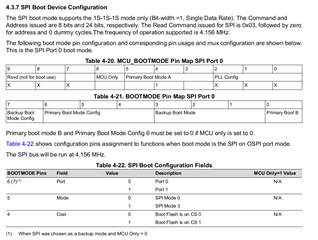
- We can find some QSPI boot configuration described in table 4-10 when MCU_ONLY=0 : "PRIMAY BOOT MODE CONFIG(6..4)" being explained as "PORT / RSVD / Csel" and Table 4-17 details PORT and Csel but we don't know what should be the value of RSVD. is it "dont'care" ? or should we force pin to '0' ? or '1' ?
- when considering SPI boot (therefore with MCU_ONLY=0 and Primary_boot_mode_B_pin=1) we can refer to table 4-11 but the required value of "BACKUP_BOOT_MODE_CONFIG" is not given

==> is it "dont'care" ? or should we force pin to '0' ? or '1' ?
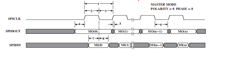
- When considering SPI boot table 4-22 gives possible selection between mode 0 and mode 3 but I could not find any chrono-diagram explaining for each mode
- which is the SPI clock edge activating Data output : rising ? or falling ?
- which is the SPI clock edge capturing Data input : rising ? or falling ?
The datasheet gives some switching characteristics (figure 6-98 to 6-103) but t is not very clear which apply to mode 0, which apply to mode 3. ==> Can you explain more ?
- When considering SPI boot we can see in table 4-1 that the only mentioned SOC peripheral is MCU_FSS0_OSPI0. However we can find in table 4-22 that either PORT0 or PORT1 can be chosen. Do you confirm that PORT1 does correspond to MCU_FSS0_OSPI1 ? which therefore should have been mentioned in table 4-1 ? or Am I mixing things ?
- When considering PCIe boot table 4-10 and table 4-46 give some possible configuration such as RESERVED / Ssc / Clocking
- Can you explain what should be the RESERVED value : don"t care ? 0 ? or 1 ?
- there is no explanation at all about "Ssc" in table 4-46. What should we conclude in that situation ? Ssc is always activated by default when booting through PCIE ? or always de-activated ?
- about "clocking" :
- what is the meaning of external pin ? do you confirm it refers to SERDESx_REFCLK (typical 100 MHz frequency )where "x" is number of the SERDES ?
- what is the meaning of internal clock ? do you suggest that PCIe clock can be elaborated from internal PLL ? in that case may be only for the Root port since other PCIe endpoint should receive external clock ? isnt'it ?
Thank you for your help
With best regards,
Bruno