Tool/software:
Hi TI Expert,
we config GPMC to synchronous NOR SRAM interface to access our FPGA's dual-port RAM.
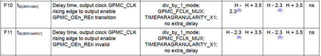
GPMC read wrong data if I set 'rdAccesstime = 2' at 133M clock, and I got correct data by either set 'rdAccessTime=3' or lower clock to like 90M.
Here's the story.
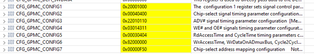
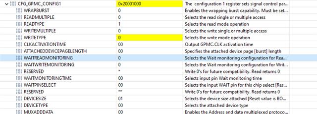
My timing setting is as following:
'.......
.timingParams =
{
.csOnTime = 0U,
.csRdOffTime = 4U,
.csWrOffTime = 4U,
.advOnTime = 0U,
.advRdOffTime = 3U,
.advWrOffTime = 3U,
.advAadMuxOnTime = 1U,
.advAadMuxRdOffTime = 2U,
.advAadMuxWrOffTime = 2U,
.weOnTtime = 1U,
.weOffTime = 3U,
.oeOnTime = 1U,
.oeOffTime = 3U,
.oeAadMuxOnTime = 1U,
.oeAadMuxOffTime = 2U,
.pageBurstAccess = 0U,
.rdAccessTime = 2U,
.wrAcessTime = 2U,
.rdCycleTime = 4U,
.wrCycleTime = 4U,
.wrDataOnMuxBusTime = 0U,
.cycle2CycleDelay = 0U,
.busTurnAroundTime = 0U,
.cycleDelaySameChipSel = CSL_GPMC_CONFIG6_CYCLE2CYCLESAMECSEN_NOC2CDELAY,
.cycleDelayDiffChipSel = CSL_GPMC_CONFIG6_CYCLE2CYCLEDIFFCSEN_NOC2CDELAY,
},
.........
snapshot of capture from FPGA side is as following:

correct data is as following

wrong data is as following

D0 and D1 data is correct
I capture the D0 and D1 pin by oscilloscope, here's the results of GPMC clock '15M' and '133M'. if 'rdAccessTime' is '2', D0 and D1 are all correct. no matter for '15M' or '133M'.
Question:
looks like while working at maximum frequency '133M', GPMC can not read correctly by setting 'rdAccessTime' to '2', even though data is physically correct.
So is there such timing restriction like 'rdAccessTime' must be larger than 2 for '133M'?