A related question is a question created from another question. When the related question is created, it will be automatically linked to the original question.
If you have a related question, please click the "Ask a related question" button in the top right corner. The newly created question will be automatically linked to this question.
DRA821U-Q1: DRA821U-Q1: SOC LPDDR4 memory controller AC timing sepcification
yes, we followed the layout guideline, we also did SI.
we looked at the spracn9f.pdf,
Most of SOC LPPDR4 memory controller timing definitions are not provided in the DRA821 LPDDR4 guidelines spracn9f.pdf, so generic Hyperlynx LPDDR4CTL.V model values were used, is this ok for simulation?
SOC documentation has provided Read RX eye uses values, however it has stated that eye width is very large (0.7 UI). If this was combined with memory device output delay uncertainties (0.3UI), meeting margin would be impossible (e.g. 0.3UI+0.7UI = 1 UI) as there would be 0 ps margin for signal transitions, jitter etc….is 0.7UI correct?
Additionally, SOC spec shows an typical RX data mask (diamond shape rather than rectangular), do you have rectangular shape?
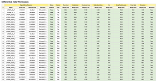
also we want you to comment on our use of memory controller timing parameters below:
SOC documentation has provided Read RX eye uses values, however it has stated that eye width is very large (0.7 UI). If this was combined with memory device output delay uncertainties (0.3UI), meeting margin would be impossible (e.g. 0.3UI+0.7UI = 1 UI) as there would be 0 ps margin for signal transitions, jitter etc….is 0.7UI correct?
Yes, my understanding is that 0.7 UI is correct. The mask is large because it needs to factor in anything not comprehended in the IBIS simulation.
You mention adding 0.3 UI for output delay uncertainties, but my understanding is that you should not need to add 0.3 UI.
As shown in the example (Figure 3-5) of the layout guidelines, there is margin when using a 0.7 UI read data mask.