Other Parts Discussed in Thread: TDA4VH, TPS6594-Q1
Tool/software:
Hello Team,
J784S4XG01EVM (TDA4AP, TDA4VP, TDA4AH, TDA4VH)
Revision: PROC141E4
PMIC: TPS6594133ARWERQ1
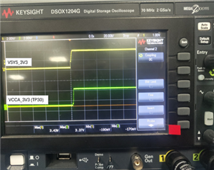
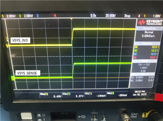
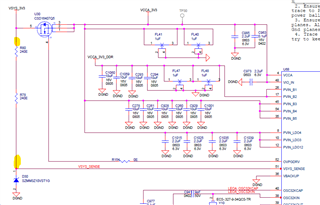
Problem Statement: We are currently using the J784S4XG01EVM board for our POC development work and have encountered a significant hardware issue following an unexpected PMIC short circuit (TPS6594133ARWERQ1) problem. After the power problem, we have observed only LD7 (VSYS_3V3), LD8(VSYS_MCUIO_3V3), LD9(VSYS_IO_3V3), only LD7 (VSYS_3V3) is enabled. since VSYS_MCUIO_3V3, VSYS_IO_3V3 is dependent on PMIC (TPS6594133ARWERQ1), we have replaced the faulty PMIC (TPS6594133ARWERQ1) and again tried to power the board. Again same issue persist, only LD7 (VSYS_3V3) is enabled. We tried to debug using the schematics all the inputs to the PMIC. we haven't found the exact root cause.
Here is our analysis:
| Pin no. | Inputs to PMIC | Signal | Dependency for to get enabled | ON/OFF | Pin no. | Outsputs from PMIC | Signal | ON/OFF |
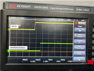
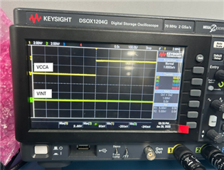
| 4 | VCCA | VCCA | - | ON | 2 | VOUT_LDOVINT | VINT_PMIC_1V8 | OFF |
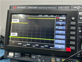
| 48 | VIO_IN | VIO_IN | - | ON | 3 | VOUT_LDOVRTC | VRTC_PMIC_1V8 | OFF |
| 26 | PVIN_B1 | PVIN_B1 | - | ON | 13 | VOUT_LDO1 | VDD_MCUIO_1V8_REG | OFF |
| 17 | PVIN_B2 | PVIN_B2 | - | ON | 11 | VOUT_LDO2 | VDD_MCUIO_3V3_REG | OFF |
| 45 | PVIN_B3 | PVIN_B3 | - | ON | 9 | VOUT_LDO3 | VDA_DLL_0V8_REG | OFF |
| 54 | PVIN_B4 | PVIN_B4 | - | ON | 7 | VOUT_LDO4 | VDA_MCU_1V8_REG | OFF |
| 35 | PVIN_B5 | PVIN_B5 | - | ON | 27 | SW_B1A | VDD_DDR_1V1 | OFF |
| 8 | PVIN_LDO3 | PVIN_LDO3 | - | ON | 28 | SW_B1B | VDD_DDR_1V1 | OFF |
| 10 | PVIN_LDO4 | PVIN_LDO4 | - | ON | 15 | SW_B2A | VDD_DDR_1V1 | OFF |
| 12 | PVIN_LDO12 | PVIN_LDO12 | - | ON | 16 | SW_B2B | VDD_DDR_1V1 | OFF |
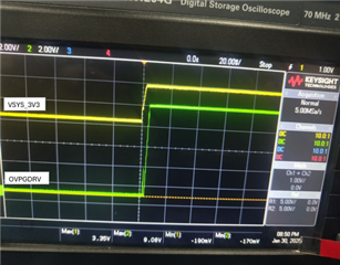
| 52 | OVPGDRV | OVPGDRV | - | ON | 43 | SW_B3A | VDD_RAM_0V85_REG | OFF |
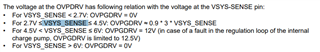
| 51 | VSYS_SENSE | VSYS_SENSE | - | ON | 44 | SW_B3B | VDD_RAM_0V85_REG | OFF |
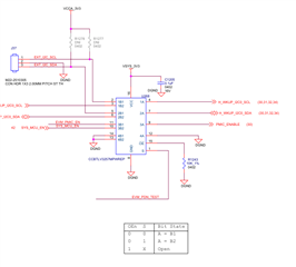
| 20 | nPWRON/ENABLE | PMIC_ENABLE | - | ON | 55 | SW_B4A | VDD_IO_1V8_REG | OFF |
| 47 | GPIO4 | SOC_PWR_WKn | - | ON | 56 | SW_B4B | VDD_IO_1V8_REG | OFF |
| 38 | OSC32KIN | LEOA_OSC32KIN | - | OFF | 34 | SW_B5A | VDD_MCU_0V85_REG | OFF |
| 46 | GPIO3 | SOC_SAFETY_ERRZ | MCU | OFF | 39 | OSC32KOUT | LEOA_OSC32KOUT | OFF |
| 18 | GPIO7 | MCU_SAFETY_ERRZ | MCU | OFF | 40 | OSC32KCAP | LEOA_OSC32KCAP | OFF |
| 41 | GPIO8 | PMIC_WDOG_DISABLE | | MAIN_PWRGRP_IRQn_BUF | PMIC Output | OFF | 1 | AMUXOUT | AMUXOUT_A | OFF |
| 42 | GPIO10 | MCU_PWRGRP_IRQn | PMIC Output | OFF | 25 | nRSTOUT | H_MCU_PORz | OFF |
| 22 | FB_B1 | VDD_DDR_1V1 | PMIC Output | OFF | 14 | nINT | H_MCU_INTn | OFF |
| 49 | FB_B4 | VDD_RAM_0V85 | PMIC Output | OFF | 29 | EN_DRV | EN_DRV | OFF |
| 50 | FB_B4 | VDD_IO_1V8 | PMIC Output | OFF | 23 | GPIO5 | EN_GPIO_RET_3V3 | OFF |
| 37 | FB_B5 | VDD_MCU_0V85 | PMIC Output | OFF | 24 | GPIO6 | EN_DDR_RET_1V1 | OFF |
| 19 | GPIO9 | EN_3V3_VIO | OFF | |||||
| 53 | GPIO11 | H_SOC_PORz | OFF | |||||
| Note: | LD7 | VSYS_3V3 | PMIC Output | ON | ||||
| LD8 | VSYS_MCUIO_3V3 | PMIC Output | OFF | |||||
| LD9 | VSYS_IO_3V3 | PMIC Output | OFF |
ON Condition: Voltage observed within default range. OFF condition No voltage observed.
we have checked all the necessary INPUT's to the PMIC. They are ON and which are OFF are dependent on the PMIC OUTPUT itself which goes to other ICs as an EN signals and from those ICs OUTPUT it comes back to PMIC IC again as an INPUT. However all the OUTPUT from the PMIC is OFF. we have also checked the power sequence for core supply VDD_CPU_AVS & VDD_CORE_OV8. They are ON.
we need your support to understand is there any software configuration & NVM settings we need to do when we replace faulty PMIC (TPS6594133ARWERQ1) when new one.
Also we need your support to understand exact root cause and to get board powered up. Please provide guidance on how to proceed with further diagnostics and potential rework.