This thread has been locked.

If you have a related question, please click the "Ask a related question" button in the top right corner. The newly created question will be automatically linked to this question.

TDA4VH-Q1: Documentation issues

Part Number: TDA4VH-Q1
Other Parts Discussed in Thread: TDA4VH, TDA4VM, TDA4VL

Tool/software:

I have downloaded the TDA4VH reference manual:

User guide J784S4 J742S2 Technical Reference Manual (Rev. D)

However there seems to be some critical information missing from the PDF.

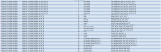
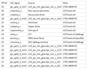
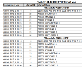
For example, I would like to see the PPI and SPI vector information for the GIC, but in the GIC section on page 804, section "9.2.1.2.2 GIC Interrupt Types" it just says:

The mapping of PPIs and SPIs can be found in section TBD .

As you can imagine, there is no "TBD" section.

Also, from what I can tell, the TDA4VH does not have an SMMU, but the documentation does say it supports PVU (peripheral virtualization unit). However on page 796, in the section 8.3.1.2 PVU Parameters, it says:

shows the PVU configuration parameters set during SoC design.

There is nothing else. The section is empty. On the other hand, in the TDA4VM manual, this section is populated.

Some related notes:

- With the TDA4VH documentation, some information is provided in the form of Excel spreadsheets. By contrast, the TDA4VM documentation is provided as PDFs only. Please note that Excel spreadsheets are much less convenient than PDFs.

- The interrupt input/output info provided in the "appedix" spreadsheet seems especially difficult to decipher.

- The PVU documentation does not show a real-world example of how to actually use the PVU. For example, if I software running on the A72 cores wanted to limit a particular DMA master so that it could only target specific RAM regions, what specific programming steps would be needed? Is there an application note somewhere that does a better job of explaining this?

-Bill

  • Hi Bill,

    The mapping of PPIs and SPIs can be found in section TBD .

    The TBD usage in the TRM is coming from the scripted automation for using the correct Section number. The GIC PPI and SPI information previously used to be part of the 9.4 Interrupt Sources chapter within the TRM.

    The TDA4VH and TDA4VL TRMs now use additional auxiliary Excel Sheets for Registers and other various items likes Interrupts, Firewalls etc. 

    The Interrupts information is now part of the Interrupts (inputs) and Interrupts (outputs) sheets of the J784S4 Appendix Excel document.

    shows the PVU configuration parameters set during SoC design.

    There is nothing else. The section is empty. On the other hand, in the TDA4VM manual, this section is populated.

    Thanks for the report, I will file an internal bug against the TRM team to fix this for the next revision.

    - With the TDA4VH documentation, some information is provided in the form of Excel spreadsheets. By contrast, the TDA4VM documentation is provided as PDFs only. Please note that Excel spreadsheets are much less convenient than PDFs.

    This is a conscious and intentional effort to reduce the size of the PDFs, and also to allow much easier searchability and filtering of the data in Excel documents.  

    - The interrupt input/output info provided in the "appedix" spreadsheet seems especially difficult to decipher.

    What are you finding it difficult? You do want to use the filtering mechanism in general to restrict the interrupts of interrest for you.

    The Interrupts (inputs) and Interrupts (outputs) sheets do present similar data from different perspectives. The Interrupts (inputs) sheet is meant to showcase the inputs into various Interrupt accepting IPs, like Interrupt Controllers, Routers, Processors etc. The Interrupts (outputs) sheet is meant to showcase the outputs generated from various peripherals.

    - The PVU documentation does not show a real-world example of how to actually use the PVU. For example, if I software running on the A72 cores wanted to limit a particular DMA master so that it could only target specific RAM regions, what specific programming steps would be needed? Is there an application note somewhere that does a better job of explaining this?

    The PVU modules are present within a VirtSS block, which is missing atm from the TDA4VH TRM. This has made the PVU chapter look like a stand-alone module. I would recommend that you leverage TDA4VM for the same. The primary usage of PVU is also with UDMA, so you would need an understanding of the DMA as well.

    The UDMA path through PVU is typically a less common usage path. I don't think there exists an App Note for this topic, but thank you for the feedback. We will strive to improve this topic for the future.

    regards

    Suman

  • What are you finding it difficult? You do want to use the filtering mechanism in general to restrict the interrupts of interrest for you.

    At the time, I wanted to figure out the set of PPI and SPI vectors assigned to the GIC for the A72 cores. I was particularly interested in how GIC vectors were being mapped to UDMA channels. (The short answer seems to be that there are ranges of SPI vectors reserved for this purpose, and you can make TI-SCI requests to set up the mappings.)

    I don't see how I'm supposed to know which entries in the input/output tables are PPIs, SPIs, or NVIC or VIM vectors. If you scroll down in the inputs table to line 209, here the Interrupt Id field seems to contain entries that correspond to the GIC SPI vectors. But unless I'm missing something, there's nothing that just comes out and tells you that. I am actually guessing that this is correct, because I looked at the TDA4VM manual, which has the PPI and SPI tables (in the section called MAIN Domain Interrupt Maps), and the TDA4VM is similar enough to the TDA4VH in this regard that I could compare the SPI table to TDA4VM spreadsheet and see where it sort of matches.

    But I don't see how I'm supposed to figure that out from the spreadsheet alone.

    The TDA4VH should have the same WKUP, MCU and MAIN domain interrupt maps as the TDA4VM manual does in its Interrupt Sources section. The inputs/outputs spreadsheet may be fine as a supplement to these maps, but it is not a replacement for them.

    I implore you to file a ticket to have these maps put back in the TDA4VH manual, and to continue to include them in future ones.

    This is a conscious and intentional effort to reduce the size of the PDFs, and also to allow much easier searchability and filtering of the data in Excel documents. 

    I'm sorry, but to me, it is not easier. I understand that in the past, some of the manuals for similar SoCs were quite large, even over 10000 pages. I sympathize with the desire to condense them, but I think the problem was more with how the information was formatted in the PDFs rather than the amount. For example, there was often repetition that could have been avoided.

    Note that PDF means Portable Document Format. In spite of what some might think, Excel is _not_ a portable file format. It's a Microsoft file format. Yes, I know there are open source office suites that support it, but you are never guaranteed 100% compatibility. And no, I don't want to open the spreadsheet using Excel on the web. I just want to read the manual. On my own computer. That's sitting right next to me. With one tool that was designed just for that purpose.

    I also don't find searching for things in Excel easier in general. Maybe if you're used to it, it might seem that way. But I want to spend my time learning how to program hardware, not Excel.

    The PVU modules are present within a VirtSS block, which is missing atm from the TDA4VH TRM. This has made the PVU chapter look like a stand-alone module. I would recommend that you leverage TDA4VM for the same. The primary usage of PVU is also with UDMA, so you would need an understanding of the DMA as well.

    The UDMA path through PVU is typically a less common usage path. I don't think there exists an App Note for this topic, but thank you for the feedback. We will strive to improve this topic for the future

    Note that my thinking here was: supposing one wants to implement a huypervisor to manage guests running on the A72 cores, and supposing one wants to allow those guests to perform DMA operations using different sets of peripherals which may be assigned to them?

    Each guest would have its own assigned region of RAM, and it's important that guests not be able to initiate DMA transfers to or from RAM that doesn't belong to them (either by accident or on purpose).

    It would also help if there was a way to transparently convert from guest physical to real physical addressing in hardware.

    Typically the Arm SMMU is used for both of those things. But TDA4VH doesn't include SMMU support. But it does have PVU and RAT. (Apparently TDA4VM has PAT instead.)

    So what I wanted to know was:

    1) Can one use PVU and/or RAT to do what the SMMU does?

    2) If so, is there a useful example that shows how?

    This would mean knowing things like how do I know what virtID values are valid and how I know how to assign them to transactions? Neither the TDA4VH nor TDA4VM manuals make this clear. An example that says "here's how you program the PVU to restrict UDMA channel X to RAM region Y" would really help.

    Note that I really do have a need for this information, so I'm a little concerned that I might have to wait until some indeterminate point "in the future" to find out.

    -Bill

  • Hi Bill,

    I don't see how I'm supposed to know which entries in the input/output tables are PPIs, SPIs, or NVIC or VIM vectors. If you scroll down in the inputs table to line 209, here the Interrupt Id field seems to contain entries that correspond to the GIC SPI vectors.

    I am not sure if you are talking about line 209 without any filtering or if you had some filtering it would change.

    Here's a snapshot after I filtered the Instance for COMPUTE_CLUSTER0_GIC500SS

    The Interrupt Input Line is clear in idenfying which is a PPI, and which is a SPI.

    the PPI and SPI tables (in the section called MAIN Domain Interrupt Maps), and the TDA4VM is similar enough to the TDA4VH in this regard that I could compare the SPI table to TDA4VM spreadsheet and see where it sort of matches.

    Indeed.

    The TDA4VH should have the same WKUP, MCU and MAIN domain interrupt maps as the TDA4VM manual does in its Interrupt Sources section. The inputs/outputs spreadsheet may be fine as a supplement to these maps, but it is not a replacement for them.

    I am sorry, but we won't be adding the tables back to the TRM.

    I'm sorry, but to me, it is not easier. I understand that in the past, some of the manuals for similar SoCs were quite large, even over 10000 pages. I sympathize with the desire to condense them, but I think the problem was more with how the information was formatted in the PDFs rather than the amount. For example, there was often repetition that could have been avoided.

    This will get a bit of used to. It also may be a case of having been used to one-style or format previously, and getting to grips with the new style.

    So what I wanted to know was:

    1) Can one use PVU and/or RAT to do what the SMMU does?

    2) If so, is there a useful example that shows how

    I recommend to fork this part of the discussion into a separate thread, so that we can get an appropriate engineer to answer those questions.

    This thread shall be used for the original Documentation issues topic.

    regards

    Suman

  • The Interrupt Input Line is clear in idenfying which is a PPI, and which is a SPI.

    When I look at this, it seems to be missing information. The SPI entries do seem reasonably accurate and informative, but the PPI entries do not. At least, they don't appear to say what someone searching for PPI vector information would need to know.

    The GIC has 16 SGIs (software generated interrupts) 16 PPIs (processor-local peripheral interrupts) and some number of SPIs (shared peripheral interrupts), which can vary depending on the silicon implementation.

    As an OS developer, I want to know which peripherals are tied to which GIC vectors, because that tells you what interrupt service routine should be used to service an interrupt when it triggers.

    PPIs are core-specific, so the expectation is to have one list for each A72 core in the SoC. The most common use for them is to trigger interrupts from the Arm generic timer that's included with the core. The timer output on each core is connected back to the CPU through a PPI input in the GIC. There is a convention that the timer uses PPIs 26 through 29 in most implementations, but I think the silicon designer may be allowed to change it (which is why the vectors are usually specified in the device tree, where they can be customized for a given platform).

    There can also be additional PPIs depending on the chip design. For the TDA4VM, we can see that PPIs 16, 22, 23, 24, 25 and 30 are also used.

    The information you showed does not seem to include the PPI vector numbers. The Interrupt ID fields are all  0. The input line description and source interrupt descriptions also don't seem to yield any meaningful information about what those interrupts are actually for. I'm not actually sure what they're trying to tell me.

    If this spreadsheet is meant to be a replacement for the interrupt map tables, then I should be able to determine the same PPI vector values and sources that match what's in the corresponding table in the TDA4VM manual (except of course where the chip design differs). If I'm being really dumb and missing it somehow, then I apologize, but I really don't see it. I've searched for all cells that include "PPI" in them, and none of the hits make any reference to the Arm generic timer.

    I am sorry, but we won't be adding the tables back to the TRM.

    Well, if I'm right and the appendix spreadsheet is indeed missing the PPI information, then I think this must be corrected somehow.

    -Bill

  • Hello,

    Scanning documents (TDA4VH+XLS, TDA4VM, + feeding documents) the PPI mapping for each of the 8 A72s looks like this:

    It is similar to what is in the PPI ID mapping table in TDA4VM's TRM but it was extended to handle the new cores.

    The TDA4VH collateral should add in the mapping table. 

    Regards,
    Richard W.
  • Sorry for the delay getting back to this, I've been stuck on a project which I've only just concluded.

    Does this means the TDA4VH documentation is indeed missing the PPI info and that TI will update it to correct this?

    -Bill

  • Hello,

    I've included the data above.  A JIRA will be filed to capture.  It would be rolled into a future manual.

    Regards,
    Richard W.
  • Ok, thank you.

    -Bill