This thread has been locked.

If you have a related question, please click the "Ask a related question" button in the top right corner. The newly created question will be automatically linked to this question.

TMS320C6678: Interfacing the ADC through the SPI with CS[2].

Part Number: TMS320C6678

Tool/software:

Hi TI Team,

I hope you are doing well.

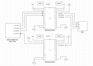
We are currently working on interfacing an ADC with the TMDSEVM6678LE using SPI communication. Since CS[0] and CS[1] are already allocated for other peripheral functions, we plan to use CS[2] for this interface.

Could you please confirm whether it is feasible to use CS[2] for SPI communication with the ADC? Additionally, we would appreciate it if you could review and suggest any necessary corrections to the attached circuit diagram to ensure proper functionality.

Looking forward to your response.

Warmest regards,

Krishn Singh Chauhan

  • Hi Krishn,

    For the TMS320C6678, the device data sheet and it says that only 2 chip selects are supported.

    For SPI connectivity, you can refer to our reference EVM schematics 

    Thanks.

  • Hi Praveen R.,

    I hope you are doing well.

    AIM: To interface an ADC with the TMDSEVM6678LE using the SPI communication protocol.

    We have referred to the schematics of the TMS320C6678 EVM Board (Rev. A101-1), TMS320C6678's datasheet, and the Technical Reference Manual (SPRUH58). Based on our major findings:

    • DSP_SSPCS0 is already allocated for the 16M SPI NOR Flash.
    • DSP_SSPCS1 is connected to the FPGA and is also configured as an INPUT on the 80-pin expansion header (TEST_PH1).

    Additionally, we reviewed the KeyStone Architecture Serial Peripheral Interface (SPI) (SPRUGP2A). This document states that the available SPI chip select signals are SPISCS[0] and SPISCS[1] (as SPISCS[n] ). However, both of these signals are currently in use.

    Given that DSP_SSPCS1 is configured as an INPUT (used for external HIGH/LOW control of the CS pins), we are uncertain how to use it as a master SPI chip select. main concerns are:

    1. Is it feasible to use DSP_SSPCS1 from the 80-pin expansion header for SPI communication with the ADC?
    2. Are there other available CS[n] lines that can be used for ADC interfacing?
    3. Is it possible to perform master-slave SPI communication with the ADC using the 80-pin expansion header, where the master can write data and read from the slave?
    4. If no additional CS lines are available, is there any recommended alternative solution, such as an I/O expander or another hardware resource?

    SPI Pins from 80-Pin Expansion Header (TEST_PH1):

    Pin No. Direction Signal Name
    63 OUT DSP_SSPMISO
    65 IN DSP_SSPMOSI
    67 IN DSP_SSPCS1
    69 IN PH_SSPCK

    Bidirectional voltage level translation with ADC using the SPI Pins (80-pin Expansion Header);

    We also use the below configurations for the SPI. In the circuit of these configurations, we want to know whether "is correct or not for that?".


    We would like to inquire about the feasibility of establishing SPI communication with an ADC using the 80-pin expansion header on the TMDSEVM6678LE. Specifically, we would like to confirm whether it is possible to:

    • Transmit data (as a master) to the ADC
    • Receive data (from the ADC as a slave)

    while maintaining proper master-slave SPI communication through the available SPI pins on the expansion header.

    We would appreciate your guidance on this matter and any recommendations for an optimal approach to successfully interface the ADC with the TMDSEVM6678LE.

    Looking forward to your valuable insights.

    Warmest regards,

    Krishn Singh Chauhan

  • Hi Krishn,

    The request info needs to be answered by a hardware/EVM expert. I will have to re-assign, so please expect a delay.

    Thanks.

  • I am sorry - I don't have access/unable to locate the TMDSEVM6678LE schematic. Could you please provide and I can review its connections.  Its mentioned a chip select connects with an FPGA.  Without knowing how the FPGA is configured, the only way to determine may be for you to assert the chip select and see how EVM responds.

  • Hi Robert E.,

    Greetings of the day.

    We sincerely appreciate Mr. Praveen R. providing us with a hardware/EVM expert to look into this matter.

    Certainly, we will provide you with the necessary documents, which we believe will help trace and resolve these issues. Please let us know if you require any additional information.

    PFA, It's  TMS320C6678 EVM Board (Rev. A101-1) (for TMDSEVM6678LE ).

    TMDXEVM6678L_EVM_A101-1_DSN.pdf

    We would appreciate it if you could review the attached circuit diagram and suggest any necessary corrections to ensure proper functionality.

    Warmest regards,

    Krishn Singh Chauhan

  • I don't have an exact answer, as I don't know exactly how FPGA is programmed and its function with using SPI.  Assuming the SPI interface is NOT required by the FPGA and board operation, you could remove R400.  This would disconnect the MISO (FPGA data output) form the SPI connection, allow you to use the SPI bus on the expansion interface (DSP_SSPCK, DSP_SSPCS1, DSP_SSPMISO, DSP_SSPMOSI) for ADC interface.

  • Hi Robert E.,

    Thank you for your support. We truly appreciate your assistance in resolving this matter. Apologies if this issue is complex, but your insights will certainly be helpful to others facing similar challenges.

    We have a few clarifications regarding the SPI interface with the ADC and the 80-pin expansion header:

    1. Impact of R400 on ADC Interfacing (for TMDSEVM6678LE ).

    • If R400 is not removed, does this mean that we cannot interface the ADC with the 80-pin expansion header? In that case, would we be unable to transmit data (as a master) to the ADC and receive data (from the ADC as a slave)?
    • If R400 is removed, we believe that we can interface the ADC with the 80-pin expansion header using the SPI pins (DSP_SSPCK, DSP_SSPCS1, DSP_SSPMISO, DSP_SSPMOSI). In this case, we would be able to transmit data (as a master) to the ADC and receive data (from the ADC as a slave). Could you confirm if this understanding is correct?

    2. DSP_SSPCS1 Pin Mode Concern

    Below is a summary of the SPI pin configuration from the 80-pin Expansion Header (TEST_PH1):

    Pin No. Direction Signal Name
    63 OUT DSP_SSPMISO
    65 IN DSP_SSPMOSI
    67 IN DSP_SSPCS1
    69 IN PH_SSPCK

    We have also observed that in the SPI circuit of the TI TMS320C6678, FPGA, NOR Flash, and 80-pin Expansion Header (TEST_PH1), there are two chip select signals: DSP_SSPCS0 and DSP_SSPCS1. While DSP_SSPCS1 operates in output mode on the DSP (TI TMS320C6678), DSP_SSPCS1 appears to function in input mode on the FPGA and the 80-pin expansion header.

    Given this configuration, we have the following key concerns:

    1. If we remove R400, DSP_SSPCS1 is set as an input on the 80-pin expansion header. In this case, would it still be possible to transmit data (as a master) to the ADC and receive data (from the ADC as a slave)? Since DSP_SSPCS1 is in input mode, could this limit its ability to function correctly in master-slave communication? Are we correct in this assumption?

    2. If DSP_SSPCS1 does not function as expected for 4-pin SPI communication with the ADC (for both Master-Slave and Slave-Master communication), would it be possible to configure the SPI in 3-pin mode and use a GPIO pin from the DSP (80-pin Expansion Header) to control the Chip Select (CS) signal (i.e., manually setting it to HIGH or LOW)? This is crucial, as we require both Master-Slave and Slave-Master communication for the ADC interface.

    3. According to our understanding, the SPI pin is configured as Slave mode only for external uses (in 80-pin Expansion Header (TEST_PH1)), Are we correct in this assumption?

    We would appreciate your insights on these points. Thank you again for your time and support.

    Warmest regards,

    Krisnh Singh Chauhan

  • The processor is the SPI master, the 80-phin expansion header (and anything plugged into it) is the SPI slave.

    DSP_SSPCK is output of processor, input to any/all slaves (including 80p header)

    DSP_SSCS1 is output of processor, input to any/all slaves (including 80p header)

    I assume you are configured for 4-pin SPI.  This configuration has separate pins for input and output.

    DSP_SSPMOSI is output of processor, input to any/all slaves (including 80p header)

    DSP_SSPMISO is input to processor, output from any/all slaves (including 80p header)


    Since the SPI interface supports 2 chip selects - the SPI master (processor) can communicate with 2 different peripherals.  For this design - you would like to have a 3 total chip select - 0/flash, 1/FPGA, 2/80p header.  But since processor only supports 2 total...will have to 'share' between FPGA and 80p.  'Share' means one peripheral (FPGA or 80p header) will have to be disabled.  By default - 80p expansion is left open, thus FPGA can use chip select without issue.  Since you want to use 80p Expansion - need to somehow disable FPGA.  I don't know how FPGA is programmed - just assuming it is using DSP_SSCS1 for SPI accesses).  

    Looking at the schematic - I don't see way to disconnect DSP_SSCS1 from FPGA.  Thus FPGA will respond when SSCS1 is asserted.  However - we can keep the FPGA from driving information onto the MISO line by removing resistor R400. 

    When processor what to communicate with 80p expansion, it will assert DSP_SSCS1 to selected slave (80p expansion and FPGA).  Processor will output CLK and DATA (MOSI) to slaves (FPGA and 80pin).  However, only the 80pin expansion can drive data back to processor on MISO (since FPGA is disconnected).