Other Parts Discussed in Thread: TMDS64EVM
Tool/software:
Hi,
We are designing a board using AM6412 where external main supply is 3V3.
Therefore VMON_SYS will come from this voltage.
Is it legal to also connect VMON_3P3_MCu and VMON_3P3_SOC to this same voltage rail ?
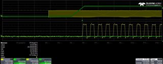
By the way the datasheet figiure 7-5 does not give any range for the timing delays during power up sequence.

What are the minimum delays ? what are the maximum delays ?
With best regards,
Bruno