Part Number: J784S4XEVM
Other Parts Discussed in Thread: SYSCONFIG
Tool/software:
Hi experts,
I am building a freeRTOS application using SDK RTOS 10.1 for the J784S4 EVM.
I am trying to route an interrupt from main GPIO0 bank0 (pin 11) to the C7x core 1.
The board is on "No boot mode" and I load my application on the c7x core 1.
I have init the pad config and the GPIO correctly. I can read the value of the GPIO0_11 when I press the SW3 button.
I have modify sciclient_defaultBoardcfg_rm.c using Sysconfig and set up the interrupt.
But I can't manage to reach the callback function.
this is my understanding of the interrupt path : 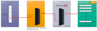
145 = GPIOMUX_INTRTR0_IN_IN_145 (=INTRTR0 input from the GPIO0 bank 0)
44 = COMPUTE_CLUSTER0_CLEC (= INTRTR output to the CLEC)
56 = GPIOMUX_INTRTR0 control register 56 setup for host C7x_0_1 by the SCIServer
440 = COMPUTE_CLUSTER0_CLEC_SOC_EVENTS_IN_IN_440 (= CLEC input from GPIOMUX_INTRTR0 56)
40 = C7x interrupt number used in the GPIO example
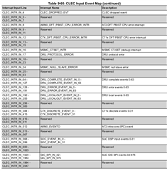
I used the "J784S4_Register_Public_20250116.xlsx" to get the following register address :
- GPIOMUX_INTRTR0
- GPIO0
- COMPUTE_CLESTER0_CLEC
using CCS memory browser view, I checked every register and they look correct.
0xa000e4 = 0x10091
0x600008 = 0x1
0x600010 = 0xFFFFFFFF
0x600034 = 0x0
0x79b81000 = 0x41100028
I can trigger the interrupt (the code reach the callback function) by writing in the CLEC send reg.
When I press the SW3 button I can see the flag in the Bank Interrupt Status Register.
I tried :
- to compile from a linux and a windows pc.
- using the OSAL and then using the CSL layer + writing in the register.
- using different pins, bank and then using the wkup GPIO module.
I have found this post which is very close to my issue, but there is no answer : J784S4XEVM: C7x GPIO Interrupt issue - Processors forum - Processors - TI E2E support forums
Thanks for your help
Charles