This thread has been locked.

If you have a related question, please click the "Ask a related question" button in the top right corner. The newly created question will be automatically linked to this question.

AM625-Q1: LPDDR4 Interface Issues on Custom AM6254 Board – Request for Support

Part Number: AM625-Q1
Other Parts Discussed in Thread: SYSCONFIG

Tool/software:

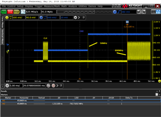
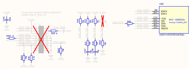
We have developed a custom board based on the AM6254ATGFHI, featuring an LPDDR4 memory interface using the ISSI IS43LQ16512A-053BLI device. All power rails for the various components are properly supplied, and the system reset signal is generated correctly. We are able to boot U-Boot from an SD card without issues.

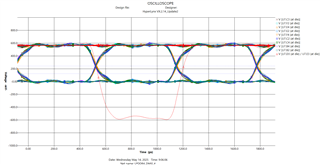
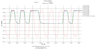
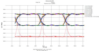
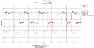
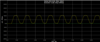
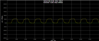
The LPDDR4 memory interface was simulated using HyperLynx, and the "DDRx Batch Simulation" passed successfully.

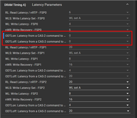
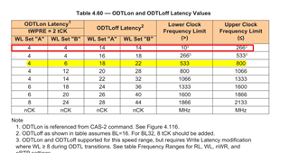
To generate the U-Boot configuration files, we used the TI SysConfig tool to create the DTSI file, based on the information provided in the memory device datasheet and the output of the signal integrity simulations.

https://dev.ti.com/sysconfig/

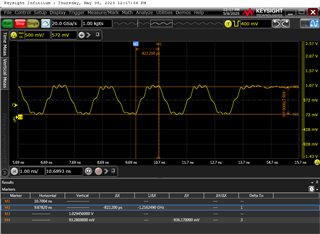
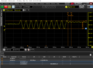
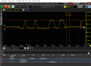
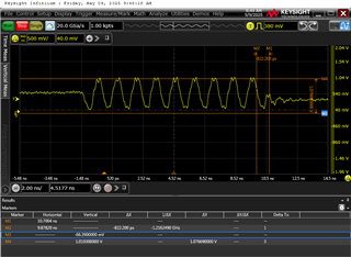
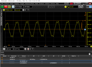
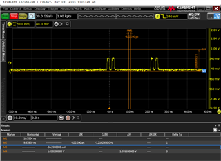
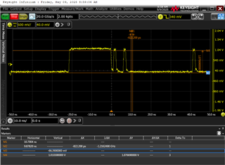
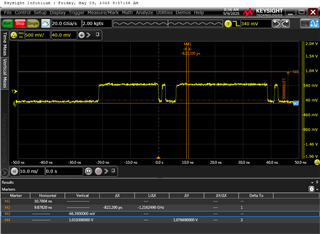
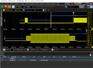
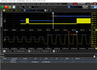
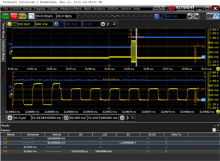
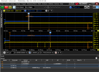
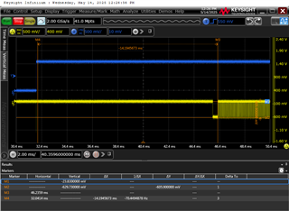
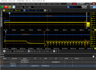
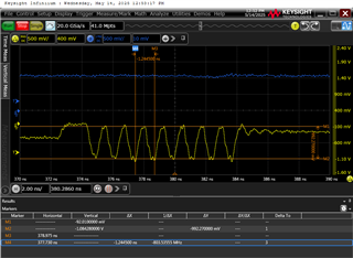
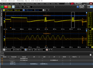
However, when booting the board and running a memory test, we observe frequent read/write errors where data appears as all zeros, instead of the expected values.

Could you provide any guidance on what we might be doing incorrectly?

Best regards.report_data.zipsettings_info_2505071627.zipSerial output UART0.txt

  • It appears you are configuring the DDR to run at 50MHz.  Is this intended?  The device has max DDR frequency of 800MHz.  Can you try changing your configuration to this frequency and test again?  

    Regards,

    James

  • Apologies, I had previously attached the configuration I was using to test some waveforms with the oscilloscope and check if they matched the simulation results. This time, I’m attaching the correct configuration, which is correlated with the memory test results.SysConfig_CPU UP 2505071555.zip

    I’ve included the waveform captured using a 3.5 GHz active probe and a 4 GHz bandwidth oscilloscope. I’m also attaching the simulated eye diagram from HyperLynx.

    The expected configuration should be a write driver (processor) with a 40 Ω pull-up/down and a 40 Ω ODT termination at the memory side. From the oscilloscope waveform, it seems that the ODT termination on the memory is not being enabled (measured amplitude is 900 mV instead of 560 mV).

  • I took a look at the changes you made in the configuration, and i believe you are changing RL, WL and nWR incorrectly.  Based on the table below from the ISSI datasheet, you should be setting them to the highlighted values

    Please try setting them back to these values and try the test again.

    As a second experiment, set WLS to "WL Set B" and test again.  This will automatically adjust RL, WL and nWR for set B values.  In the past, i believe the ISSI memories required this setting to enable ODT at 800MHz operation.  

    Regards,

    James

  • Hi,

    We’ve performed the tests you mentioned, but the terminations are still not being activated on the data, strobe, and other lines… and, as expected, we are seeing errors in the memory tests. I’m attaching several waveforms: the signal measured on DQ15, near the memory pin, using the new configuration, differential DQS0, DMI0... It’s surprising that sometimes the CA lines appear to have the ODT terminations active for several seconds, while at other times they do not...The CS signal does appear to have its ODT termination active.

    CS signal... it seems to have its ODT active:

    The CA0... signals sometimes have ODT active and sometimes not…

    This behavior seems extremely strange to me, but I’m not sure to what extent the hardware could be influencing it. We have checked the 240 Ω calibration resistors, and they are correct.

    I’m attaching an image of the schematic for the LPDDR4 interface. I haven’t found anything abnormal. I’ve reviewed the component footprints and pin assignments multiple times, and I haven’t found anything unusual.

    LPDDR4 INTERFACE.pdf

  • From the register dump in your serial output, it appears that training is failing, so that is probably why the signal swing doesn't look correct. 

    How did you come up with the termination and drive strength settings, especially the ones you changed in the Register Config Tool?  Did these come from simulations?  

    I'd like to try to start with the minimal amount of changes to the default configuration.  I kept your bit swizzle information, and just changed a few timing parameters based on the ISSI datasheet. Can you load up the attached .syscfg to generate a new configuration to try.  If this still fails, please provide the regdump like you did before.

    REgards,

    James

    https://e2e.ti.com/cfs-file/__key/communityserver-discussions-components-files/791/Min_5F00_changes.syscfg

  • Hi,

    The DTSI file was generated using the Min_changes.syscfg configuration file, with only the timing parameters for the IS43LQ16512A-053BLI memory modified.
    However, the output appears unchanged.


    The modified Min_changes.syscfg file and a terminal dump of the UART0 output are attached.

    There is some uncertainty regarding the ODT latency parameters.


    The IS43LQ16512A-053BLI memory appears to require an ODTLon latency of 4 clock cycles and an ODTLoff latency of 18 clock cycles when operating at 800 MHz.
    At 50 MHz, however, the required ODTLon latency remains at 4 clock cycles, while the ODTLoff latency is reduced to 14 clock cycles. In contrast, Micron memories such as the MT53E1G16D1 (used on the EVB) seem to support ODTLon and ODTLoff latencies of 0 cycles at 50 MHz.

    Nonetheless, the SysConfig tool sets both ODTLon and ODTLoff to 0, which appears to be incorrect for the IS43LQ16512A-053BLI device.

    Furthermore, analysis of the generated DTSI file reveals a possible lack of consistency between the DENALI_CTL and DENALI_PI register values.

    This raises the question of whether such inconsistencies could prevent the ISSI memory from functioning properly in the intended configuration.

    Regards.

      7484.dump.txt 

    0451.k3-am62x-ddr-config_minchanges.dtsi.txt

  • Hi,

    The ODT termination values for the data, CA, CLK, DQS... were obtained through post-layout simulation using HyperLynx.

    Here some examples (the simulation results don't account for the delay introduced by the controller on the DQS signals relative to DQ, nor on the CLK signals relative to CA.

    1) CA/CS/CLK lines:

    2) DQ[7:0]/DM0/DQS0 lines (write)

    3) DQ[7:0]/DM0/DQS0 lines (read)

    4) DQ[15:8]/DM1/DQS1 lines (read)

    4) DQ[15:8]/DM1/DQS1 lines (write)

    The report generated by HyperLynx, which confirms that the simulation results are valid, is also included.

    DDR_Report.zip

    Regards.

  • Hello,

    several oscilloscope traces captured during the LPDDR4 initialization sequence are also included. After the first rising edge of CKE, two CLK bursts can be observed. The first operates at 50 MHz (presumably used for memory initialization), while the second continues at approximately 800 MHz.

    A zoomed-in view of the 50 MHz burst is provided.

    After a certain period, ODT termination is observed to be enabled on the CLK signals. That's right.

    The duration of this 50 MHz pulse burst (presumably used to configure the ISSI LPDDR4 memory registers) is approximately 5.43 µs.

    Prior to that time, pulses are already present on the CA1 line, where ODT termination is observed to be inactive. Note that the differential probe is inverted, so the waveform is also displayed inverted.

    After approximately 14.195 ms, the ODT signal on the CA1 line appears to be active, indicating that it has been properly configured.

    The following figures shows the behavior observed on the DQ5 data line.

    After approximately 18.281 ms, activity appears on the data bus.
    Note that the differential probe is inverted, so the waveform is also displayed inverted, similarly to the previous CA case.

    Some spurious pulses are observed on DQ5 prior to this point (three in totat,but they do not appear to be significant).
    A zoomed-in view is provided to examine the initial pulses on the DQ5 line in greater detail.

    The DQ5 data line does not have ODT termination enabled.


    The hypothesis is that the incorrect activation of ODT termination on the DQ lines leads to a failure in the subsequent training process. As a consequence (and also due to the absence of active ODT termination) a high number of memory access errors are observed.

    Regards.

  • Hi Amilcar,

    thank you for the details.  The regdump is still showing that training is not completing correctly. 

    When i attached min_changes.syscfg, i meant for you to try this without any other changes.  I believe this should match the timings specified in the ISSI datasheet.  You are correct that i did miss the ODTLon/off timings, but i don't think at this point that is causing the training failures.  Typically these are disabled (ie, set to 0) for the boot frequency.  Even the ISSI datasheet mentions that if they are enabled for the lower frequencies, you would have to have WL>8.  All memories we have worked with (including ISSI at other customers) worked fine with ODTLon/off=0 at the boot frequency

    We have to take a step by step approach with small changes to better understand why training is failing.

    1. Try with min_changes.syscfg without any other changes.  Post regdump.

    2. Try with 1) plus adjust "Termination: CA ODT(FSP2)" to 40ohm to match your simulation results.  Post regdump.

    3. Try with 2) plus adjust "ODT Pull-Down DQ/DM" and "Termination: SOC ODT (FSP2)" to 40ohm to match your simulation results.  Post regdump.


    I took a look at your scope shots.  I believe so far every thing is as expected, and since the training doesn't complete correctly, any kind of a transaction will potentially fail.  But most of the first portion of the training is operating as normal.

    Regards,

    James

  • Hi,

    We are sending you the dump file containing the UART output for each of the three cases.

    1. min_changes.syscfg without any other changes.  Post regdump.

    dump_min_changes.txt7041.k3-am62x-ddr-config.dtsi.txt

    2. With 1) plus adjust "Termination: CA ODT(FSP2)" to 40ohm to match your simulation results.  Post regdump.

    dump_min_changes Termination CA ODT FSP2.txt7041.k3-am62x-ddr-config.dtsi.txt

    3. With 2) plus adjust "ODT Pull-Down DQ/DM" and "Termination: SOC ODT (FSP2)" to 40ohm to match your simulation results.  Post regdump.

    dump_min_changes Termination CA ODT FSP2 ODT PullDown DQDM and Termination SOC ODT FSP2.txt7041.k3-am62x-ddr-config.dtsi.txt

    The waveforms provided in the previous post were captured after the memory controller completed the configuration of the ISSI memory registers. It is understood that the training process begins at this point. During training, delay lines and Vref values are adjusted; however, the ODT settings programmed in the memory device are not modified.

    Based on the voltage levels observed on the DQ5 line (which are representative of the other data lines as well), it is clearly evident that ODT is not being activated. Therefore, it remains unclear how the training process could complete successfully under these conditions.

    The DQ5 signal is shown following LPDDR4 memory configuration, during the initial access cycles.
    In these accesses, the CA and CLK signals do have termination enabled.  The captured signal is compared against simulation results. The approximate signal amplitude can also be inferred from the pull-up/down strengths of the driver and from the presence or absence of ODT termination. For a more accurate estimation, the current tables from the IBIS model may be consulted.

    With ODT termination enabled at 40 Ω during calibration, the expected signal amplitude (at the same measurement point used with the oscilloscope) should be:

    The signal amplitude obtained from HyperLynx simulation closely matches the estimated value calculated based on the driver's output current characteristics and the 40 Ω ODT termination value.

    Regards.

  • Hi Amilcar, apologize for the delay.

    The regdumps are still showing CA VREF training is failing for each of the three cases.  This is one of the first training steps that occurs, and without this, the rest of the training will not work. There is something fundamental that is not right, but I'm not sure what it is at the moment.

    I'm actually really surprised that you were able to boot to uboot (as mentioned in your original post).  If you remove the regdump and memtester, can you boot to uboot everytime?  Are you able to boot to kernel?

    I've asked our FAE to arrange a call so we can further discuss. 

    Regards,

    James


  • Hi,

    Apologies if my initial post was unclear. What I meant is that U-Boot was booting from the SD card and attempting to access the LPDDR4 bus. As expected, U-Boot does not complete the process and ends up hanging.  If weremove the regdump and memtester, the result doesn´t change.We will coordinate with our FAE to prepare for that call.


    In the meantime, what additional tests or oscilloscope measurements could we perform to get more information that might help find the root of the issue?

    Regards.

  • Hi,

    I can´t fully understand what mechanism could be causing the CA Vref training process to fail.
    I can see that the CA signals activate their ODTs and are properly aligned with the CLK signal…
    However, since the DQ ODTs are not enabled (and I know you've mentioned this is expected), the only possibilities that come to mind are: either the internal memory registers are not being correctly programmed, or they are being reset at some point, or possibly being overwritten.

    Is there any way to investigate any of these three possibilities using the oscilloscope?

    Regards.

  • The issue is happening very early on during Command Bus Training.  There is a point where the controller sweeps the CA VREF across a range to train to the optimal value.  What is strange is that this training resolves to a value of 0, even though the start/stop points that it is supposed to check are non-zero.  It almost seems like the controller is not communicating with the memory properly, or some of the initial MR writes are not working. (as you suggest). I don't think there is anything to observe with a scope during CA VREF training.     

    -Is this happening on multiple boards?

    -Is this also happening on a board without any probes attached?  Maybe the probes are having an effect on the training.  

    -have you tried with a memory device from a different manufacturer?

    -is the memory device soldered to the board, or is the some sort of interposer you are using to access the signals?

    -Do you have JTAG header on the board?

    Regards,

    James

  • Hi, James,

    the issue has been observed on the first six prototypes assembled with ISSI IS43LQ16512A memory devices.
    This thursday, we will test three additional prototypes using MICRON's MT53E1G16D1 memories.

    We're not currently using JTAG, although the connector is populated on the PCB (but remains unused).
    The issue occurs even when no oscilloscope probes are connected to the board.
    The memory device is directly soldered to the simulated PCB, without any interposer.

    Do you think that the presence of the unconnected JTAG header on the board could be interfering with the LPDDR4 interface?
    How would you suggest we verify this?

    I send you an image of the JTAG section as implemented in the schematic.

    Regards.

  • Hi Amilcar,

    no, i don't think the JTAG header would have any affect on the LPDDR4 interface.  The reason i was asking is that it might be a little easier to debug if we had this installed.  We could perform DDR init or MR reads using GEL scripts and the Code Composer debugger.

    I think the experiment with the Micron memory will be very useful.  If you can get similar regdumps before the call, we can compare those on the call.

    Regards,

    James

  • Hi, James,

    we've identified the issue we had. The initial training process was failing. For the CA Vref calibration, the processor sends bit patterns on the CA[0:5] lines which are mirrored for reading on DQ[8:13].

    When verifying how the "bit swizzle" of the DQ[8:13] lines was configured in the SysConfig tool, I noticed we had misinterpreted how to set it up.

    We are currently running initial tests on our boards, and everything seems to be functioning correctly.

    Thanks.