This thread has been locked.

If you have a related question, please click the "Ask a related question" button in the top right corner. The newly created question will be automatically linked to this question.

AM5728: Inquiry on PCIe EP Outbound Configuration Method

Part Number: AM5728

Tool/software:

Hello,
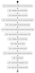
I am currently working on configuring PCIe Endpoint (EP) using the AM5728, with a Windows-based PC set as the Root Complex (RC). I am developing an example in which data is transmitted from the AM5728 to the PC using an outbound configuration.

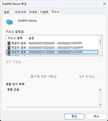
At present, the base address of the outbound window is set to the internal RAM of the AM5728 (0x4040_0000), and the target address is configured to the physical address of BAR2 on the Windows side, as shown in Device Manager (0x7410_0000).

After writing data to the internal RAM and triggering EDMA for transmission, I expect the data to be updated on the PC side. However, the data does not appear to be updated.

For reference, I have confirmed that the inbound configuration (on a different BAR region) is working correctly.

I would appreciate your assistance in reviewing and correcting the outbound settings.

  • Hello DaeWon,

    Can you please share what SDK version you are using? Are you using Linux?

    -Josue

  • Currently, we are using the <processor_sdk_rtos_am57xx_09_03_00_00 / pdk_am57xx_1_0_21> PDK and have configured a bare metal-level SBL as a separate project, using only the board, csl, drv, and osal libraries. We are not using TI-RTOS or Linux.

  • The value currently entered corresponds to the selected region in the figure, which is 0x7410_0000 (BAR2).

  • Hi DaeWon,

    Can you try to do a flush for the cache on the AM57-side before triggering the EDMA. And then do an invalidate of cache on the Windows PC-side before reading the memory?

    Just want to make sure the data is not stuck in cache, and that the data is propagated properly to memory.

    Regards,

    Takuma

  • I have implemented an example that performs data exchange in the sequence shown in the diagram.
    On the EP side, cache invalidation is performed. On the PC side, cache invalidation was not applied, as it is generally not required in this case.
    After triggering the EDMA on the EP side, I also confirmed that no errors were reported in the error status registers.
    I will try applying cache invalidation on the PC side as well.

  • Hi DaeWon,

    I will try applying cache invalidation on the PC side as well.

    Just in case. 

    Reviewing the sequence diagram, for troubleshooting the issue, are there checks put in place for verifying if EP read the BAR2 address correctly from BAR0 in the third block from the top, and checks to confirm EP correctly wrote to BAR2 address in the block that is four up from the bottom?

    Regards,

    Takuma

  • To verify whether the physical address of BAR2, which was read through BAR0, is correct, communication needs to be established. Therefore, we are currently reading the value directly via the debug port.
    As a result, we have confirmed that the address matches the one output by the device driver, and we are proceeding by using that address as the target address.
    Additionally, regarding the cache invalidation on the PC side that you mentioned — it seems that Windows does not provide explicit support for this.
    If you know of an alternative method, we would appreciate it if you could share it with us.

  • Hi DaeWon,

    I am not too savvy with Windows method for handling cache. However, I can point to some material for Linux:

    Specifically, this slide:

    And this slide:

    As for some experiments, can you try writing without EDMA? If direct CPU writes work, then it will make EDMA set up and cache a bit more suspicious.

    Regards,

    Takuma

  • diagram Link

    I haven't yet been able to proceed with the cache invalidation on Windows as you suggested, since I haven't found a working method for it.

    Additionally, I tried performing an outbound (OB) transfer without using DMA, by directly writing data to the target's BAR2 physical address. However, this caused the firmware to fall into an exception state.

    As a reference, I’m sharing a block diagram of the PCIe initialization code I’ve written. The configuration values—especially for the outbound window—have been included in the diagram. If you notice anything incorrect or misconfigured, I’d really appreciate your feedback.

  • Hi DaeWon,

    Additionally, I tried performing an outbound (OB) transfer without using DMA, by directly writing data to the target's BAR2 physical address. However, this caused the firmware to fall into an exception state.

    This is a bit unexpected. It should be possible to read/write without using DMA, although it will be a bit less efficient... unless there is a limitation in hardware that makes it necessary to use EDMA to package up the data into a format understandable by PCIe.

    In any case, there are a couple of old application notes for PCIe which has some example pseudo code for setting up PCIe and doing transfers via EDMA. If you have not read through them, I would recommend reading through them and comparing with your code:

    CTRL+F for "example" and that should point you to the locations scattered around in the app notes that have the examples.

    Regards,

    Takuma

  • After reviewing the datasheet and the CSL loopback example, I discovered that I had overlooked the PCIE_SS1 region.
    The CSL example sets BAR0 for both inbound and outbound transfers, and it is confirmed to be a loopback example.
    In this example, the BAR is configured as follows:

    [BAR0 Config]
      locationParam.location = PCIE_LOCATION_LOCAL;
      locationParam.outboundCfgOffset = OUTBOUND_CFG_OFFSET;

      barParams.barAddrSize = PCIE_BAR_ADDR_SIZE_32BIT;
      barParams.barType = PCIE_BAR_TYPE_MEMORY;
      barParams.enableBar = PCIE_CONFIG_ENABLE;
      barParams.enablePrefetch = PCIE_CONFIG_ENABLE;
      barParams.lowerBarMask = INBOUND_PCIE_LIMIT;
      barParams.lowerBaseAddr = INBOUND_PCIE_ADDRESS; // (0xA0000000) External Memory
      barParams.upperBarMask = PCIE_UPPER_ADDRESS;
      barParams.upperBaseAddr = PCIE_UPPER_ADDRESS;

    [BAR0 Outbound]
      locationParams.location = PCIE_LOCATION_LOCAL;

      regionParams.regionDir = PCIE_ATU_REGION_DIR_OUTBOUND;
      regionParams.tlpType = PCIE_TLP_TYPE_MEM;
      regionParams.enableRegion = PCIE_CONFIG_ENABLE;

      regionParams.lowerBaseAddr = OUTBOUND_MEM_SPACE; // (0x05000000) PCIE_SS1 Offset??
      regionParams.upperBaseAddr = PCIE_UPPER_ADDRESS;
      regionParams.regionWindowSize = OUTBOUND_MEM_SPACE_LIMIT;

      regionParams.lowerTargetAddr = OUTBOUND_PCIE_ADDRESS; // (0xB0000000) External Memory
      regionParams.upperTargetAddr = PCIE_UPPER_ADDRESS;

    [BAR0 Inbound]
      regionParams.regionDir = PCIE_ATU_REGION_DIR_INBOUND;
      regionParams.tlpType = PCIE_TLP_TYPE_MEM;
      regionParams.enableRegion = PCIE_CONFIG_ENABLE;
      regionParams.matchMode = PCIE_ATU_REGION_MATCH_MODE_BAR;
      regionParams.barNumber = 0;

      regionParams.lowerBaseAddr = INBOUND_PCIE_ADDRESS; // (0xA0000000) External Memory
      regionParams.upperBaseAddr = PCIE_UPPER_ADDRESS;
      regionParams.regionWindowSize = INBOUND_PCIE_LIMIT;

      regionParams.lowerTargetAddr = RX_DATA_BUFFER_ADDR; // (0x90000000) External Memory
      regionParams.upperTargetAddr = PCIE_UPPER_ADDRESS;

    My question regarding this example is:
    Although this is a loopback example, how can the address mapping be adjusted if I want to implement an example where the RC is the PC and the EP is the AM5728?

  • Hi DaeWon,

    For PC as RC and EP as AM5728, have you referenced section "5 PCIe Programming Example" of https://www.ti.com/lit/an/sprabk8/sprabk8.pdf ?

    There should be two separate examples, one for RC and another for EP. I presume the EP-side example can be followed for AM5728, while the RC-side you can develop a similar application as the one in the application note.

    Regards,

    Takuma