This thread has been locked.

If you have a related question, please click the "Ask a related question" button in the top right corner. The newly created question will be automatically linked to this question.

AM6442: GPMC and NOR Flash Switching Characteristics

Guru 10085 points
Part Number: AM6442

Tool/software:

Hi Support Team,

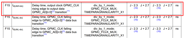
I would like to confirm the AM6442 datasheet: Table 6-55. GPMC and NOR Flash Switching Characteristics - Synchronous Mode.


My customer is developing a board with AM6442 and is trying to set timing restrictions (setup, hold) in FPGA.
In the above specification, J = GPMC_CLK, so at 50MHz, this would be 20ns.
In this case, Min = 17.7ns and Max = 22.7ns, so is it correct to expect the valid data width is between 17.7ns and 22.7ns?
Unlike other specifications, this one only specifies TRANSITION time, so let me check just to be sure.

Best Regards,
Kanae

  • Hello Kanae

    Thank you for the query.

    Let me reassign the query to our GPMC expert to support.

    Regards,

    Sreenivasa

  • Hi Sreenivasa,

    Thank you for your reply.

    I understand that your GPMC expert will help me with this matter.
    I would appreciate a prompt response.

    Best Regards,
    Kanae

  • Hi Kanae,

    I want to clarify what the data sheet switching characterization table communicates.
    Each data may be launched slightly ahead or slightly behind the clock edge that it launches on. Since one bit may be ahead and another bit may be behind, the customer needs to assume the worst case when performing timing analysis.
    It is also important to understand what the "F15" notes describe - after the first data, all data is launched on the falling clock edge (and assumed to be latched on the rising clock edge). These are "half-cycle timings" where the clock pulse width is used for timing analysis instead of the clock period. Refer to the three figures below that show data launched early, data launched nominally, and data launched late.

    Assuming a perfect clock (which is inadequate)
    worst tSU = 20/2 - 2.7 = 7.3ns
    worst tH = 20/2 - 2.3 = 7.7ns

    Factoring in the datasheet limits of the clock pulse width from F1 in the Switching Characteristics table...
    Min pulse width = 0.475P - 0.3
    worst tSU = 9.2 - 2.7 = 6.5ns
    worst tH = 9.2 - 2.3 = 6.9ns

    The customer should also factor in PCB propagation delays of clock verses each data and subtract the worst difference from setup time and hold time. For example, If clock is a shorter trace than the longest data then there is less setup time and the difference must be subtracted from the setup time calculation.

    Data Launch: Early

    Data Launch: Nominal

    Data Launch: Late

    Regards,
    Mark

  • Hi Mark,

    I appreciate your explanation of the details.
    I did not understand the notes.

    Is my understanding correct that note (11) First transfer only for CLK DIV 1 mode. of “F15” td(clkH-do), which I have asked about this time, is limited, so basically, it should be set by considering notes (12) and (13) of other “F15” td(clkL-do) and assuming worst-case scenarios?

    Best Regards,
    Kanae

  • Hi Kanae,

    I should have explained notes 11, 12, 13 further.

    (11) is for first transfer only with GPMC_CLK divide-by-1 from GPMC_FCLK: data launches on rise edge of GPMC_CLK, but well ahead of the rising edge clock that latches that data (when WEn is asserted also).

    (12) is for 2nd, 3rd, 4th, etc. data with GPMC_CLK divide-by-1 from GPMC_FCLK - data launches on falling edge of GPMC_CLK (using half cycle timings) after first data has launched on rising edge

    (13) is for all data with GPMC_CLK in divide-by-2, -3, or -4 from GPMC_FCLK - all data launches on the falling edge of GPMC_CLK (using half cycle timings) 

    Is my understanding correct that note (11) First transfer only for CLK DIV 1 mode. of “F15” td(clkH-do), which I have asked about this time, is limited, so basically, it should be set by considering notes (12) and (13) of other “F15” td(clkL-do) and assuming worst-case scenarios?

    Right - the setup time for first data is easier to satisfy as it has an additional half clock cycle when compared with 2nd, 3rd, 4th, etc. data which is (half cycle timing). However, the hold time for first data is defined by note (12) - half cycle timing, assuming worst case scenarios.

    Make sure that the WEn timing does not trick the memory into latching the first data twice - as first data is driven on rise edge and could be on the bus many rising edges before second data, the setting of WEn must be calculated to tell the memory when to begin latching the first data. WEn can be launched on rise edge or falling edge using the WEExtraDelay bit. Setup and hold time of the WEn must similarly be calculated for worst case.

    Regards,
    Mark

  • Hi Mark,

    Thank you for your support!

    Let me check again.
    In the case of the first F15 (td(clkH-do)), is it safe to calculate with J=GPMC_FCLK
    as it is described in the data sheet as follows, so there is no need to make it half-clocked?
    Or is it necessary to consider the worst case and make it half-clocked in this case as well?

    F15: td(clkH-do)
    Delay time, output clock GPMC_CLK rising edge to output data GPMC_AD[n:0](1) transition(11)

    Mark said;.
    However, the hold time for the first data is defined by note (12) - half cycle timing, assuming worst case scenarios.

    Let me also confirm the above.
    If note (12) affects the first F15 (td(clkH-do)), it would be easier to understand
    if note (11) and (12) were also included in F15 as shown below, or if “J/2 - 2.3 J /2 + 2.7” were included in the definition.

    F15: td(clkH-do)
    Delay time, output clock GPMC_CLK rising edge to output data GPMC_AD[n:0](1) transition(11)(12)

    Best Regards,
    Kanae

  • Hi Mark,

    Thank you for your support.

    I need to report back to my customer, could you please reply back when I will be able to get your answers?

    Best Regards,
    Kanae

  • Hi Kanae,

    I'm having a hard time understanding the questions. But I'll try to answer.

    In the case of the first F15 (td(clkH-do)), is it safe to calculate with J=GPMC_FCLK

    Yes - for the first data with divide-by-1 clock, it is accurate to calculate setup time from data launch on CLK rising edge to data latch on CLK rising edge. In divide-by-1 clock mode, only the first data launches on the bus at the rising CLK edge. All other data launches on a falling CLK edge.
    My suggestion is that if the setup time is satisfied for half-cycle (data launch on falling edge, latch on rising edge) then it should be satisfied for full clock cycle also.

    Let me also confirm the above.
    If note (12) affects the first F15 (td(clkH-do)), it would be easier to understand
    if note (11) and (12) were also included in F15 as shown below, or if “J/2 - 2.3 J /2 + 2.7” were included in the definition.

    Hold time for the first data is defined by when the second data appears on the bus. Since second data launches on the falling clock edge then the hold time for the first data must be satisfied before the falling clock edge, when the second data launches. This is why the hold time for first data depends on note 12. The second data may launch as early as 1/2 FCLK - 2.3ns after rising CLK edge that latches data at the memory. The first data must be considered invalid at 1/2 FCLK - 2.3ns minus any other worst case timings like CLK to data PCB delay mismatch, where data travels faster than the CLK on the PCB.

    Regards,
    Mark

  • Hi Mark,

    Thank you for your reply.

    I will share it with my customer.

    Best Regards,
    Kanae