This thread has been locked.

If you have a related question, please click the "Ask a related question" button in the top right corner. The newly created question will be automatically linked to this question.

TDA4AEN-Q1: GPIO

Part Number: TDA4AEN-Q1

Tool/software:

Hello,

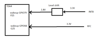
    I got some issue about GPIO configure, below is hardware configure, we configured both wake up GPIO66/GPIO79 as input, wakeup GPIO 66 is working correctly, when it is applied 3.3V, read as"1", when it is applied 0v, read as "0", but wakeup GPIO79, whenever 0V or 1.8V applied, both read as "0", because wakeup GPIO79(P25) is ADC power domain, we applied ADC power domain(VDDA_ADC0/VDDA_ADC1, J21/K21) to 1.8V. does it need to some configure for 1.8V level input(like enable some level shift etc. because they are in same GPIO bank)

Thanks.

Jiang Liu

  • Hi Jiang,

    Have you taken a look at the following documentation regarding ADC pins?

    The ADC pins can be configured and used for WKUP_GPIO0_[79:86], however, they are not selected via the MUXMODE field to select the signal. Instead it does done by setting the MCU_ADCn_CTRL_GPI_MODE_EN bit to one within the CTRL_MMR_CFGn_MCU_ADC0_CTRL register. Additionally, they can only be used as GPI or general purpose input signals.

    Thanks,

    Neehar