This thread has been locked.

If you have a related question, please click the "Ask a related question" button in the top right corner. The newly created question will be automatically linked to this question.

AM62A7-Q1: AM62A OSPI NAND ensure data reliability

Part Number: AM62A7-Q1
Other Parts Discussed in Thread: UNIFLASH

Tool/software:

Vaibhav, 

Based on our last meeting, the use of OSPI NAND was proposed as a cost-saving measure. However, we need evidence to ensure data reliability, especially regarding the boot firmware. Please provide documentation or test results that explain how data integrity is maintained when using AM62A with OSPI NAND—such as boot protection mechanisms, ECC, wear leveling, etc.

[FAQ] AM62A7: Bad Block Implementation for NAND Flash Parts - Processors forum - Processors - TI E2E support forums

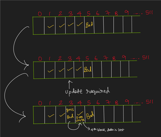
Specific bad block management has what features, such as data storge in flash bad blocks, whether this part of the data is directly lost. The other is whether the code can still be started if there is a bad block of the address.I can see we can support BBM on the ROM code but I need more details how to confirm that the binary stored in the NAND will not be loss. It can ensure still be boot normally. 

  • Hi,

    Please allow me sometime to put forward an explanation.

    Thanks,

    Vaibhav

  • Hi,

    Here is my explanation which you can put forward to the customers.

    I would like you to refer my FAQ as well which you have referenced in the query description.

    Apart from this, I have discussed with the ROM team and confirmed that bad block management is indeed supported.

    So lets say, while doing uart uniflash you are supposed to flash an image at a certain offset. Suppose this offset falls at a block which was bad, hence the next good block will be used to flash the image.

    Assuming ROM was supposed to boot from this certain offset, then ROM will also take care of the bad block and consider the next good block(where the desired image is stored) to boot from.

    So in summary, BBM is supported while booting and for application as well.

    Hope this clarifies your doubts in conjunction with the call we had today.

    Regards,

    Vaibhav

  • Vaibhav,

    It's still not clearly that if some data storage in the block. But when will bad block occur and at that time what will happen? Like At that time data will loss or it will copy to next good block?

  • Hi,

    Allow me sometime to provide you a detailed breakdown again.

    Regards,

    Vaibhav

  • Hi Kangjia,

    Before reading further, please make a note of the following:

    Bad blocks happen during write and erase cycles. Read operation never causes a bad block.

    On this note, I am assuming a process where the binaries are firstly written to the flash. This is carried by a simple UART uniflash process.

    Lets pick 3 scenarios:

    Goal: To flash the binary at offset 0xOFFSET. Assume 0xOFFSET falls at Block 5 and ROM needs to boot from this flashed binary.

    • First Scenario:
      The block 5 is good and the binary is flashed correctly to the same block. Now ROM will boot properly from the block 5.

    • Second Scenario:
      The block 5 is already bad, hence the binary is flashed to the next good block(lets say Block 6 is the next good block). Now, when ROM boots, it expects the binary to be at block 5, but since it knows block 5 is bad, it picks the next good block to boot from which in this case is Block 6.

    • Third Scenario:
      In this case, block 5 is good, but while writing the binary assume the block 5 went bad, then the write operation will fail, hence.

    Does this cover the details needed by the customer?

    Regards,

    Vaibhav

  • Hi Vaibhav,

    Thanks for the reply.

    Today customer discussed with the GD supplier about the support for NAND-related issues under abnormal conditions. For normal conditions, they can support bad block management. In the case of sudden power-off (since customer has a project that only supports K15 power supply, and the software cannot receive the corresponding signal during unexpected power loss), if there was previously a flash erase/write operation (such as firmware upgrade, EDR, or log writing), it is likely to cause data damage in the data area. GD mentioned that such situations require system-level software support.

    Hence, customer is asking us if we have a solution for this scenario? The current board does not have a capacitor-based snubbing solution.

    Thanks,

    Kevin

  • Hi Kevin,

    In the case of sudden power-off (since customer has a project that only supports K15 power supply, and the software cannot receive the corresponding signal during unexpected power loss), if there was previously a flash erase/write operation (such as firmware upgrade, EDR, or log writing), it is likely to cause data damage in the data area. GD mentioned that such situations require system-level software support.

    Let me analyze this and get back to you in sometime.

    Regards,

    Vaibhav

  • if there was previously a flash erase/write operation (such as firmware upgrade, EDR, or log writing)

    Please let me know if the writing process is going to be via the UART Uniflash script which TI provides or is it some external tool like JTAG, Gang Programmer and so on?

  • Hi Vaibhav,

    I will first elaborate on the usage scenarios: This refers to a scenario where the device is already installed, and during the customer's usage process, logical bad blocks occur due to sudden power loss when writing logs, EDR, or FOTA upgrades. The system has self-healing capabilities to address these issues. This is not a scenario involving manual connection to a serial port or JTAG interface.

    Thanks,

    Kevin

  • Hi Vaibhav,

    Seeing from the below thread last sentence, we have on-die ECC support for OSPI/QSPI Nand. May I know how does this ECC function & could it be used to resolve the concern for the power loss situations? Do you think a "super-capacitor" is still a must requirement to have even if we have ECC support?

    https://e2e.ti.com/support/processors-group/processors/f/processors-forum/1467194/am625-enable-gpmc-nand-ecc-and-bad-block-for-gpmc-nand-chip-in-sdkla-v10-01-10-04/5632464?

    Thanks,

    Kevin

  • Hi Vaibhav,

    We have discussed with GD & customer again today to deep dive the bad block protection in a sudden power off situation.

    GD mentions in a sudden power off situation, whether or not a page/block will be labeled as a bad block is decided by SoC side. Hence, GD & customer need TI provide a specific logic that how we label a bad block. However, as seen from our FAQ, we just mentioned that we only judge if a block is bad block according to the value of first page 128 bytes spare area (if it is oxff). We did not mention how we label or under which situation we change the 0xff to a different value.

    Hence, may I know that when bad block happens, it is the NAND Flash HW itself changes the first page spare area to a value other than 0xff, not SOC did this right?

    Thanks,

    Kevin

  • We have discussed with GD & customer again today to deep dive the bad block protection in a sudden power off situation.

    GD mentions in a sudden power off situation, whether or not a page/block will be labeled as a bad block is decided by SoC side. Hence, GD & customer need TI provide a specific logic that how we label a bad block. However, as seen from our FAQ, we just mentioned that we only judge if a block is bad block according to the value of first page 128 bytes spare area (if it is oxff). We did not mention how we label or under which situation we change the 0xff to a different value.

    Hence, may I know that when bad block happens, it is the NAND Flash HW itself changes the first page spare area to a value other than 0xff, not SOC did this right?

    Hi Kevin,

    Allow me sometime to comment on this.

    Regards,

    Vaibhav

  • Hi Vaibhav,

    GD double confirms that our SOC identifies bad blocks during operation by determining that a block has experienced bit flips exceeding the ECC error correction capability, or is unable to be erased or written to. In such cases, the block is deemed unreliable for data storage and is marked as a bad block.

    Hence, customer wants to know that in the case that during the OTA, the power loss happens when writing some pages inside a block (which means the writing process is not finished), then will SOC mark it as a bad block?

    Thanks,

    Kevin

  • Hi Vaibhav,

    To be more specific for the above question, when we writing to the NAND Flash, is our SOC doing ECC checking for each page inside a block or we only do ECC checking after all the pages have been written within a block. The point is when the power loss situation happens it is more likely that we are writing a page and there are still some pages in the block have not been written yet. If we do ECC checking for each page we write, then it could be more likely we will label bad block right?

    Thanks,

    Kevin

  • Hi Kevin,

    Vaibhav is out of office today. But I can summarize my discussion with the experts on this.

    1. Bad block marker (non 0xFF) value written by the SoC.

    2. The identification of a "new" bad block (which is not tagged yet, but has gone bad) happens when the SoC tries to write/erase to the flash and that operation doesn't complete successfully. At this point, the SoC writes the spare area i.e. 1st byte of the 1st page in the block by a non 0xFF value.

    3. Upon every boot, the SoC creates a local list of bad blocks in an array by reading the spare area. This array gets updated when any new bad block is identified.

    4. Support for tagging bad blocks based on the ECC on the NAND flash is not supported today in the software, the mechanism which I explained in point 2 is what is used today.

    Now coming to the specific scenario when during a firmware update, if the power loss happens, the write to a page in the block may still be in flight. This may or may not cause a bad block. In case when it does create a bad block, upon the next boot whenever you try to re-write to the same block, below will happen.

    1. SoC boots and creates an array of known bad blocks by reading the spare area. The block which turned bad during the last failed firmware update is still not tagged.

    2. During the new write cycle, SoC tries to write to the same block which had turned bad due to a power loss during an in flight write in the last firmware update cycle.

    3. Write fails on this block, SoC writes the spare area for that block by a non 0xFF block (marking it bad) and updates its local array for bad blocks.

    4. SoC jumps to the next good block and writes the same data. This is the bad block management logic where you try to write the data to the next good block.

    Regards

    Karan

  • Hi Karan,

    Thanks for this detailed explanation, we understand it now.

    Based on this information, we know that when the block we are writing is turns bad we will write to the next good block, but the next good block may already have some data so the overwritten will happen.

    If this understanding is correct, then if customer uses Nand flash and OTA is required, customer may need reserve additional spare spaces for each of the SW components right? Because if two SW components/image address in Nand Flash are quite close to each other then the overwritten situation could affect the next good SW image.

    Then for considering this scenario, do we have some suggestions to the customer? As in automotive project OTA is normally required, and we do see Nand Flash is more cost effective which may save the BOM cost and give us more competitively to win the project.

    Thanks,

    Kevin

  • Hi Kevin,

    If this understanding is correct, then if customer uses Nand flash and OTA is required, customer may need reserve additional spare spaces for each of the SW components right? Because if two SW components/image address in Nand Flash are quite close to each other then the overwritten situation could affect the next good SW image.

    Yes, the process of finding the next good block to write doesn't check if the good block is free or not. So the system integrator will need to pad with "a few" (depending on the amount of bad blocks acceptable, the grade of the flash, the firmware size requirements etc.) blocks when designing the memory layout for the NAND flash.

    Function to find the next good block: https://github.com/TexasInstruments/mcupsdk-core-k3/blob/k3_main/source/board/flash/ospi/flash_nand_ospi.c#L1634 

    Regards

    Karan

  • Hi Karan,

    Thanks for providing this details, I have discussed with customer that in the most of cases padding few blocks will work, but there could be a special situation that this may still have some concern.

    In most cases

    Customer re-flash the entire SW image, for example, the SW image will be written to block 1-10, and block 5 is bad block, then according to our bad block management logic, we will actually write block 1-4, & 6-11. Then if customer pad block 11 in their design this will not have any problem.

    In special case

    There is a SW component or some important data that have already been saved in block 1-4, during the runtime, customer may only update a part of the important data, let's say re-writing to block 3, then if bad block happens, according to our bad block logic, the block 4 will be overwritten, and this seems padding few blocks method will not work in this situation.

    Customer discussed with me that to resolve the above special case, could we modify our bad block management logic a little bit that every time we try to write to a new good block we check if that is empty or not and until we find the empty block.6

    However, i think if we modify our logic like this, it will affect the above "in most cases" result, as we will write to block 11 for the data which originally will write to block 5, and results that the block 6 data will write to block 12.

    May I know how do you think about this?

    Thanks,

    Kevin

  • Hi Kevin,

    In special case

    There is a SW component or some important data that have already been saved in block 1-4, during the runtime, customer may only update a part of the important data, let's say re-writing to block 3, then if bad block happens, according to our bad block logic, the block 4 will be overwritten, and this seems padding few blocks method will not work in this situation.

    Customer discussed with me that to resolve the above special case, could we modify our bad block management logic a little bit that every time we try to write to a new good block we check if that is empty or not and until we find the empty block.6

    However, i think if we modify our logic like this, it will affect the above "in most cases" result, as we will write to block 11 for the data which originally will write to block 5, and results that the block 6 data will write to block 12.

    May I know how do you think about this?

    I understand the special case/edge case. Allow me sometime to revert back to this with an explanation.

    Regards,

    Vaibhav

  • Hi Vaibhav,

    Any progress to share please? We will onsite customer with our marketing team this Wednesday to discuss this.

    Kevin

  • Hi Kevin,

    The current SDK flow is as following:

    Notice, how the 4th block is overwritten with the updates made to block 3. Since block 3 went bad we write to the block 4 as block 4 is good.

    Currently in the SDK we do not check if the block we are writing to is already having some binaries flashed. This is expected by the customer to take care of.

    So the implementation from the customer's end should be to just add a check if the next block is good and there is no binary flashed already, hence we write to it.

    Regards,

    Vaibhav

  • Hi Vaibhav,

    Thanks for the reply.

    Based on the above case, if customer adds a check if the next block is good and there is no binary flashed already. Then, the 4th block which goes bad will be written to block 6. And then, we we write a next data, will it be written to block 7 or 4?

    Based on this theory, if customer wants to reflash an image which covers block from 0 to 99, customer has to erase the original image before flashing the new image right? If customer did not do it, then once a bad block happens in the middle, and if customer implements a check if the next block is good and there is no binary flashed already, then the original image will not be fully written by the new image.

    Thanks,

    Kevin

  • Hi Kevin,

    Based on the above case, if customer adds a check if the next block is good and there is no binary flashed already. Then, the 4th block which goes bad will be written to block 6. And then, we we write a next data, will it be written to block 7 or 4?

    I think you meant when the 3rd block goes bad and we want to update the binary in the 3rd block, then in this case, since:

    4th is good but has binary so we skip

    5th is bad so we skip

    6th is good and has no binary, hence the update is made here.

    Based on this theory, if customer wants to reflash an image which covers block from 0 to 99, customer has to erase the original image before flashing the new image right? If customer did not do it, then once a bad block happens in the middle, and if customer implements a check if the next block is good and there is no binary flashed already, then the original image will not be fully written by the new image.

    This is a correct understanding, before writing to any block, erase should be performed on that block, this will follow up a write operation.


    Let me know where you need more clarifications?

    Regards,

    Vaibhav