This thread has been locked.

If you have a related question, please click the "Ask a related question" button in the top right corner. The newly created question will be automatically linked to this question.

DRA829J: Functional clock for R5F subsystems from MAIN domain

Part Number: DRA829J

Tool/software:

Dear TI-Team,

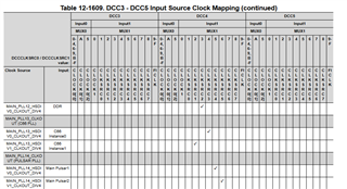
While checking the TRM for the functional clock sources of R5FSS0 and R5FSS1, we realized that in the integration diagram there's a CTRL_MMR0 register to select the clock source.
However, when checking the table with the corresponding options, there's only a single value. Also, we didn't find any register to select clock source for R5FSS0 and R5FSS1.
Either diagram is wrong or table needs to be updated. See pictures below:

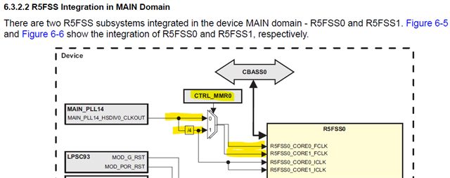
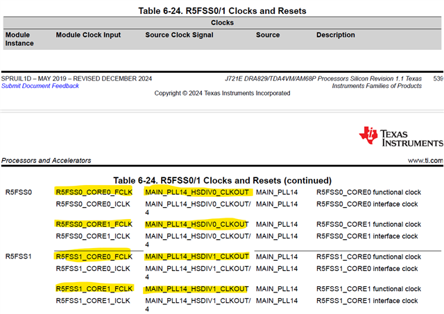
Can you please check and confirm which is the correct information?

Thank you in advance.

Regards,
António

  • Hi Antonio,

    Either diagram is wrong or table needs to be updated. See pictures below:

    I can confirm that the diagram is wrong (looks to be a copy-paste and modified from MCU R5FSS). The MCU R5FSS does have a valid CTRL_MMR register for choosing a functional clock of 333 MHz (recommendation would still be run this at 1000 MHz), but there is no such selection logic for MAIN R5FSS0 and MAIN R5FSS1 instances. They are indeed expected to run at 1000 MHz, with the Interface Clock running at 250 MHz clock.

    The divide-by-four for the MAIN_PLL14_HSDIV0_CLKOUT does supply the ICLK, and is also provided for DCC Monitoring of this MAIN_PLL14 HSDIV clocks.

    regards

    Suman

  • Thanks Suman for your confirmation.
    Now it's clear for us.