This thread has been locked.

If you have a related question, please click the "Ask a related question" button in the top right corner. The newly created question will be automatically linked to this question.

AM69: Timing requirements for Power Supply Sequencing

Part Number: AM69

Tool/software:

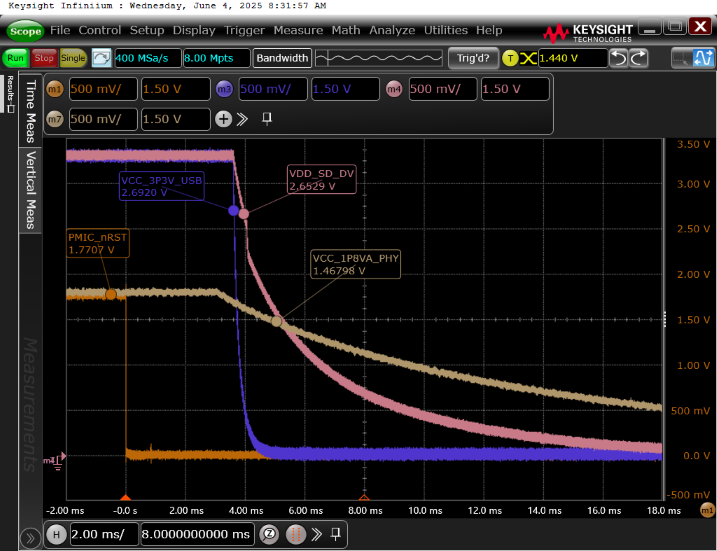
Section "6.10.2Power Supply Sequencing" in the datasheet describes various power supply sequences and specifies time stamps that indicate approximate elapsed times.

For example, section "6.10.2.2 Combined MCU and Main Domains Power-Up Sequencing" specifies time stamps as follows.

• T0 – 3.3V voltages start ramp-up to VOPR MIN. (0 ms)
• T1 – 1.8-V voltages start ramp-up to VOPR MIN. (2 ms)
• T2 – Low voltage core supplies start ramp-up to VOPR MIN. (3 ms)
• T3 – Low voltage RAM array voltages start ramp-up to VOPR MIN. (4 ms)
• T4 – OSC1 is stable and PORz/MCU_PORz are de-asserted to release processor from reset. (13 ms)

I understand that the time stamps are approximate and not strict timing requirements.

Can the times indicated by the time stamps be ignored?

Best regards,

Daisuke

  • The recommended power up seq is required. The time stamps are reference examples that are not absolute requirements. Your design can have different time stamps values as long as they align to the power sequence timing.

  • Hi Bill-san,

    Thank you for your reply.

    I understand that only the order specified by timestamps in the power-up / down sequences is required.

    During power-up, each power rail is required to turn-on after the power rails defined by the earlier timestamps has ramped-up and stabilized.
    During power-down, each power rail is required to turn-off and ramped-down before the power rails defined by the later timestamps.

    As long as the above conditions are met, are different turn-on/off times and ramp-up/down times allowed for power rails defined by the same timestamp?
    So, can any of the power rails be supplied from different power supplies?

    Our customer uses two different power supplies for the 3.3V power rails (T0) on their custom board.
    There is a relatively long delay between the two 3.3V power rails.

    Is this relatively long delay (282.237ms) between the two 3.3V power rails acceptable?

    The power connections and delays during power-up are as follows.

    3.3V power rails (T0):
    VDDSHV0_MCU,VDDSHV1_MCU,VDDSHV0,VDDSHV2 (0s)
    VDDSHV5, VDDA_3P3_USB (282.237ms)

    Analog 1.8V power rails (T1):
    VDDA_1P8_SERDES, VDDA_1P8_USB (283.931ms)
    Others (283.991ms)

    Digital 1.8V power rails (T1):
    VDDSHV2_MCU, VDDS_MMC0 (284.21ms)

    Low voltage core supplies (T2):
    VDDA_0P8_PLL_DDR, VDDA_0P8_DLL_MMC0 (284.876ms)

    The order in which the power rails are ramped-down during power-down on their custom board is incorrect.

    Is it acceptable for the order in which the power rails ramp-down to be incorrect?

    The power connections and delays during power-down are as follows.

    MCU_PORz & PORz assert low (T0):
    MCU_PORz, PORz (0s)

    Low voltage core supplies (T2):
    VDDA_0P8_PLL_DDR, VDDA_0P8_DLL_MMC0 (1.611ms)

    Digital 1.8V power rails (T3):
    VDDSHV2_MCU, VDDS_MMC0 (2.825ms)

    3.3V power rails (T4):
    VDDA_3P3_USB (3.287ms)
    VDDSHV5 (3.601ms)

    Analog 1.8V power rails (T3):
    VDDA_1P8_SERDES, VDDA_1P8_USB (4.918ms)

    Best regards,

    Daisuke

  • Hi Bill-san,

    Thank you for your support. Our customer is waiting for your reply.

    Please give me an answer as soon as possible. Your prompt reply would be appreciated.

    Best regards,

    Daisuke

  • Hi Bill-san,

    The order in which the power rails are ramped-down during power-down on their custom board is incorrect.

    Is it acceptable for the order in which the power rails ramp-down to be incorrect?

    Some of the analog 1.8V power rails (T3), such as VDDA_1P8_SERDES and VDDA_1P8_USB, start to ramp-down before the 3.3V power rails (T4), but due to the slower ramp-down time, they turn-off later than the 3.3V power supply (T4).

    Is this acceptable?

    Best regards,

    Daisuke

  • Hi Bill-san,

    Thank you for your support. I am sorry for posting repeatedly. Our customer is waiting for your reply.

    Please give me an answer as soon as possible. Your prompt reply would be appreciated.

    Best regards,

    Daisuke

  • Hi Bill-san,

    Thank you for your support. I am sorry for posting repeatedly. Our customer is waiting for your reply.

    Please give me an answer as soon as possible. Your prompt reply would be appreciated.

    Best regards,

    Daisuke

  • Hi Bill-san,

    Thank you for your support. I am sorry for posting repeatedly. Our customer is waiting for your reply.

    Please give me an answer as soon as possible. Your prompt reply would be appreciated.

    Best regards,

    Daisuke

  • The present power up sequence that applies 3.3V to a few SoC inputs and then has >200ms time delay before additional input supplies are energized is subjecting the SoC to a "partial power state". TI does not characterize SoC reliability for "partial power state". It is recommended to apply all SoC input supplies in a concise power up sequence that approximates the time stamps shown in the data manual. Any risk associated with SoC POH reliability when using a non-standard power up sequence will be on the customer to validate and support.

    Present power down sequence that asserts MCU_PORz 1st followed by disabling of SoC inputs supplies as shown is good.