This thread has been locked.

If you have a related question, please click the "Ask a related question" button in the top right corner. The newly created question will be automatically linked to this question.

DRA821U: User Guide for Powering JacintoTM 7 J7200 DRA821 with Single TPS6594-Q1 PMIC, PDN-2A

Part Number: DRA821U
Other Parts Discussed in Thread: DRA821

Tool/software:

Hello,

I am using an DRA821 processor and implementing the single PMIC power scheme using the document  "slvucd4.pdf".

The question I have is the pull-up power rail for GPIO6. 

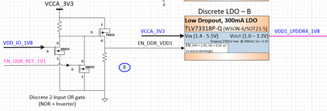
The document refers to this signal as name as EN_DDR_RET_1V1, and suggests the pull-up power rail to be VDD_DDR_1V1_REG.

This is used to enable an LDO to provide the power rail VDD1_LPDDR4_1V8.

This would mean that the DDR 1V1 rail would precede the DDR 1V8 rail.

I think this is a mistake.

LPDDR4 requires the 1V8 rail to be powered BEFORE the 1V1 rail.

NOTE: I DO NOT intend to use DDR retention in my design.

Q1/ Can I enable the DDR 1V8 LDO with the power rail VDD_IO_1V8 (PMIC LDO1) ?

Q2/ Instead can i wire the power rail VDD_IO_1V8 (PMIC LDO1) directly to the DDR4 1V8 pins ?

Q3/ How should I wire up the CPU pin DDR_RET (ball # R5) ?

Thanks,

Steve

  • 0, The DRA821 PDN-2A scheme uses a discrete OR gate in order to allow the EN_DDR_RET_1V1 control to keep the VDD1_DDR_1V8 supply energized during DDR Retention low power mode. The VDD_IO_1V8 supply is the 2nd input to the OR gate and it is responsible for both power up & down sequencing.

    1. & 2. Yes, if you are not using DDR Retention, then VDD_IO_1V8 alone can be used to control VDD1_DDR_1V8 LDO.

    3. Install a 10k pull-down resistor connected to R5 (DDR_RET) if you do not intend to use DDR Retention. 

  • Hello Bill
    Is the reference schematic you are mentioning above available to download for DRA821 and PDN-2A?
    Thank you and best regards
    Stephan