This thread has been locked.

If you have a related question, please click the "Ask a related question" button in the top right corner. The newly created question will be automatically linked to this question.

TDA4AL-Q1: Timing Parameters for LPDDR4 Interface

Part Number: TDA4AL-Q1

Tool/software:

Hello Team,


We are using TDA4AL-Q1 processor in one of our design & would like to do Signal Integrity simulation for LPDDR4 interface with 4266MT/ps data rate.

So, we need timing specification values for the below mentioned parameters for TDA4AL processor. Currently, TDA4AL datasheet doesn't have timing specifications for LPDDR4 interface.

Output timing Parameters:

  • tCKCA, tCKCS, tCKCKE : CA, CS, CKE prelaunch delay relative to CK (both min & max values)
  • tDQSDQ: DQ/DM prelaunch delay relative to CK (both min & max values)
  • tCKDQS: DQS delay relative to CK

Input timing Parameters:

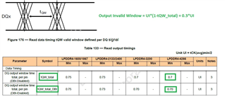
  • VdIVW(mV), TdIVW1(UI), TdIVW2(UI): Data Read eye masks parameters values(min).
  • TdiPW(UI): Minimum Read Data Oulse Width
  • VIHL_AC_DQ(mV): addition to eye mask if any additional requirement for the signal to reach a minimum peal level.

Please do the needful ASAP.

Best Regards,

Hoysalachar N N

  • Hi,

    Please refer to the layout and routing guidelines application note which provides information on performing simulations.

    https://www.ti.com/lit/pdf/spracn9

    Regards,
    Kevin

  • Hi Keven,

    Thanks for your input, we are considering this App Note for designing the PCB.

    But for signal Integrity simulation, we need above timing requirements to verify the simulation results at TDA4AL. It is important for us to simulate & verify LPDDR4 interface with such higher data rate of 4266MT/s data rate.

    Please do the needful, thanks!

    Best Regards,

    Hoysalachar N N

  • I'm sorry but we do not provide any timing parameters for the LPDDR4 controller.  All required design parameters are specified in the previous mentioned application note.

  • Hello Escler,

    Thank you for the feedback. 

    The App Note SPRACN9 has design parameters for LPDDR4 eye mask. But I have concern on eye width requirement of 0.7*UI for data rate 4266MT/s.

    For Data read, as per JEDEC the Output Invalid window is 0.3*UI for LPDDR4 memory chip(below image FYR). The TDA4AL requires 0.7*UI eye width(TdIVW) which is not possible if we consider 0.3*UI invalid window for LPDDR4 memory DQ signals as PCB will also add some jitter. So, below are few queries please provide your feedback ASAP.

    1. Is this 0.7*UI eye width(TdIVW) requirement for TDA4AL is excluding DRAM memory Invalid Window of 0.3*UI ?

    2. If I need to include DRAM memory Invalid window(0.3*UI), then there should be some relaxation from 0.7*UI requirement for PCB. Could you please confirm ?

    Below are the screenshots from JEDEC specs & TDA4AL APP Note on above concerns.

    JEDEC spec:

    TDA4AL TdIVW requirement from APP NOTE:

    Best Regards,

    Hoysalachar N N

  • Hello Team,

    We are waiting for your feedback, could you please check & get back to on the above concern.

    Best Regards,

    Hoysalachar N N

  • Hi,

    My understanding is that you do not need to add 0.3 UI to the read mask. 

    Regards,
    Kevin

  • Hi Kevin,

    Thank you for the feedback.

    Regards,

    Hoysalachar N N