This thread has been locked.

If you have a related question, please click the "Ask a related question" button in the top right corner. The newly created question will be automatically linked to this question.

TDA4VE-Q1: In TDA4VE SOC,The gpio pin is configured as pull_up, the actual measured output is only about 0.9V

Part Number: TDA4VE-Q1

Tool/software:

Hello TI engineers,

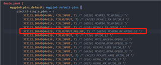
We are currently using the TDA4VE and have a problem configuring the multiplexed pins of the GPIO. We configured gpio0_10 as the power-up enable control for USBVBUS, and configured the pin in the device tree as shown:

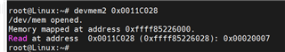
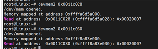
We measured the state of the pin after configuration and found that its output is only 0.9V

This is our hardware connection diagram:

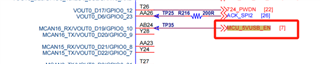
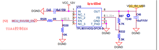
MCU_5VUSB_EN is the pin we want to control.

  • Hi Bruce,

    Could you please share a register dump for the respective PADCONFIG register? 0x0011C028

  • Hi  Mark,

    This is the value of the register:

    I checked the register definitions in the datasheet and didn't find anything unusual about this value。

    Regards

  • Hi Bruce,

    Thanks for the register dump—I agree this value is normal. In a baremetal test case on our EVM where the PADCONFIG register is programmed to this value, I observe the pin pull up to rail as expected.

    I think the internal pull-up resistor may be creating a voltage divider with the external R529+R530 resistors in your schematic.

  • Hi Mark,

    R529 is a 0R resistor and R530 is a 10K resistor.As shown in the hardware schematic I pasted above:

    We tried to disconnect R529 and directly measure the level state of the TDA side of the MCU_5VUSB_EN pin (measuring the TP35 test point level) and found that the pin did output 3.3 V. But once the R529 resistor was reconnected, the output of this pin changed back to 0.9V~1V.
    Similarly, we tried disconnecting this pin from R529 and replacing it with a different GPIO pin connected to R529 to control the EN of the TPL8051, and strangely enough, all the voltage states were normal after replacing it with the other pin. I also read the register value of this pin and it is exactly the same as 0x0011c028. Only MCU_5VUSB_EN (AB24) is not normal. Is there anything else about this pin that needs special configuration?

    Regards

  • Hi Bruce,

    That is strange behavior. With the pullup enabled on T26, I would expect to see a similar divided voltage due to the R530 pulldown resistor. AB24 does not need any additional configuration to use the internal pull-up resistor.

    Can you please confirm where you measured when T26 was connected to R529?

  • Hi Mark,

    When we use T26 to go to R529, we have disconnected MCU_5VUSB_EN (AB24) from R529. So the points we are measuring are the T26 pin(3.3V), the voltage value on the left side of R529(3.3V), and the voltage value of the TD40(5V) in the diagram above.

  • Thanks for clarity on where is measured. Is R530 still connected in this case? With R530 connected, I expect it there to be a voltage drop. Without R530, I expect it to be 3.3V.

    Bruce, could you please try disabling the transmitter via PADCONFIG (set Bit 21) on both pins and report the voltages you observe?