This thread has been locked.

If you have a related question, please click the "Ask a related question" button in the top right corner. The newly created question will be automatically linked to this question.

AM62A7-Q1: How to RD (Read) DQ Calibration in Nanya DRAM?

Part Number: AM62A7-Q1
Other Parts Discussed in Thread: AM62A7

Tool/software:

Hi,expert
Environment:
    SOC:AM62A7-Q1
    DRAM:Nanya NT6AN256T32AC-J1H
Question:
    For functional safety, we need to check the connection of DRAM pins (DQ). The following are the steps for DQ in Nanya datasheet:
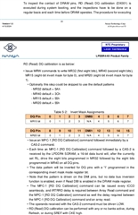
We did not find the relevant register in the AM62A7 TRM. How can we RD (Read) DQ calibration?
Best regards,
XUE Fadong
  • Hi Xue,

    There are a few registers which allow the user to read/write MR registers in the memory.  Here are some example GEL functions which should be easily adapted to C code.  The functions will only work if the DDR controller/PHY are properly initialized and trained.

    Wait()
    {
    unsigned int i;
    for(i=0;i<10000;i++);
    }

    Check_and_Ack_MRW()
    {
    while((HW_RD_REG32(CTL_BASE + DDRSS_CTL_351__SFR_OFFS) & 0x8) == 0x0)
    Wait();
    HW_WR_REG32(CTL_BASE + DDRSS_CTL_359__SFR_OFFS, 0x8); //ack the status mode bit
    Wait();
    }

    Check_and_Ack_MRR()
    {
    while((HW_RD_REG32(CTL_BASE + DDRSS_CTL_351__SFR_OFFS) & 0x4) == 0x0)
    Wait();
    HW_WR_REG32(CTL_BASE + DDRSS_CTL_359__SFR_OFFS, 0x4); //ack the status mode bit
    Wait();
    }

    hotmenu MR_Write(unsigned int mr_addr,unsigned int cs, unsigned int data)
    {
    HW_WR_REG32(CTL_BASE + DDRSS_CTL_190__SFR_OFFS,((1UL << 23) | (cs << 8) | mr_addr));
    Wait();
    HW_WR_REG32(CTL_BASE + DDRSS_CTL_225__SFR_OFFS, data );
    //trigger write
    Wait();
    HW_WR_REG32(CTL_BASE + DDRSS_CTL_190__SFR_OFFS, ((1UL << 25) | (1UL << 23) | (cs << 8) | mr_addr)); //set bit 25 to write
    Wait();
    Check_and_Ack_MRW();
    GEL_TextOut("Writing %x to MR%d\n",,,,,data,mr_addr);

    }

    hotmenu MR_Read(unsigned int mr_addr,unsigned int cs)
    {
    HW_WR_REG32(CTL_BASE + DDRSS_CTL_190__SFR_OFFS, ((cs << 8) | mr_addr) << 8 ); //CS0 MR0
    HW_WR_REG32(CTL_BASE + DDRSS_CTL_190__SFR_OFFS, ((1UL<<16) | (cs << 8) | mr_addr) << 8 ); //trigger read
    Check_and_Ack_MRR();
    return(HW_RD_REG32(CTL_BASE + DDRSS_CTL_192__SFR_OFFS));

    }


    Regards,

    James