

Other Parts Discussed in Thread: SYSCONFIG, AM62A3, AM62P, AM62D-Q1
Tool/software:
Hi TI Experts,
Could you please elaborate about PADCONFIG register bits and default configurations for PADCONFIG registers.

This thread has been locked.
If you have a related question, please click the "Ask a related question" button in the top right corner. The newly created question will be automatically linked to this question.
Hi Board designers
Thank you for the interest.
The FAQ is being updated.
Please review the FAQ frequently for updates.
Available device packages
Example PADCONIG register bit description - AM62L
Example PADCONIG register s default value summary - AM62L
Regards,
Sreenivasa

Hi Board Designers,
Input regarding PADCONFIG registers:
General note on PADCONFIG
Many of the device IOs are turned off by default and external pull resistors may be required to hold inputs of any attached device in a valid logic state until software initializes the respective IOs. The state of configurable device IOs are defined in the BALL STATE DURING RESET RX/TX/PULL and BALL STATE AFTER RESET RX/TX/PULL columns of the Pin Attributes table. Any IO with its input buffer (RX) turned off is allowed to float without damaging the device. However, any IO with its input buffer (RX) turned on shall never be allowed to float to any potential between VILSS and VIHSS. The input buffer can enter a high-current state which could damage the IO cell if allowed to float between these levels.
PADCONFIG ST_EN
The minimum Input Slew Rate parameter defined in each Electrical Characteristics table is associated with long-term reliability. These parameters are not a function of the ST_EN bit. Note: We never expected software to disable hysteresis on any of the input pins. This is a mistake that needs to be fixed.
The minimum Input Slew Rate parameter defined in each peripheral timing section is a requirement to meet the respective peripheral timing parameters.
The device may not work as expected if you violate the minimum input slew rate limit defined in the respective peripheral timing section, but the device could be permanently damaged if you violate the minimum input slew rate limit defined in the respective Electrical Characteristics table. It is very important that you minimize the time a signal connected to one of our input buffers spends in the mid-supply region as it transitions from low to high or high to low.
Several of the AM62x GPIO have an internal debounce circuit in their path to the GPIO module, which can be configured to filter a noisy signal. This would be a better solution than applying an external RC filter that slows the signal slew rate. See Note1 attached to each GPIO Signal Description table in the datasheet to know which GPIO inputs have the debounce feature. GPIO1_30 does not have the debounce capability.
The Schmitt Trigger function implemented in the input buffer only changes the output results of the input buffer, by filtering noise pulses that do not exceed the hysteresis.
The Schmitt Trigger function does not change how the input buffer is compromised when a system applies a slew rate to its input that is slower than defined in the datasheet.
The product must be designed to be in compliance with our datasheet requirements. If not, the non-compliance could reduce the life of the AM62x device.
couldn't find a way to configure ST_EN bit using our SysConfig tool. Is that a missing feature?
Meanwhile got feedback from the SysConfig team:
Yes, we are currently working on adding multiple additional PADCONF settings in SysConfig in the future releases (including ST_EN and others see below list). Also these will come up depending on the register reset and how the pad is defaultly set. Again here is the list of new settings that will appear in the tool with per pin specific configuration at reset.
Groups (additional settings):
- WAKEUP:
WKUP_EN
WK_LVL_POL
WK_LVL_EN
- DSLEEP:
DS_PULLTYPE_SEL
DS_PULLUD_EN
DSOUT_VAL
DSOUT_DIS
DS_EN
- ISO:
ISO_BYP
ISO_OVR
Main (basic settings):
- PULLTYPESEL
- PULLUDEN
- RXACTIVE
- ST_EN
- DEBOUNCE_SEL
- DRV_STR
(+) AM62A3: eMMC and USB_VBUS questions - Processors forum - Processors - TI E2E support forums
AM62A3 buffer enable, which has an over-ride called TX_DIS (bit 21) in the respective PADCONFIG register. You need to keep that bit set until MUXMODE (bits 3-0) is set to select the appropriate signal function. The output may glitch if you leave the output buffer enabled while changing the value of MUXMODE. The external pull will hold the logic state while the output buffer is disabled.
there is no Padconfig register for MMC0_* and OLDI0_*
The pins associated with MMC0 and OLDI0 do not have PADCONFIG registers.
(+) [FAQ] AM623: MMC0 HS200 slew rate - Processors forum - Processors - TI E2E support forums
Regards,
Sreenivasa
Hi Board Designers,
Input regarding PADCONFIG registers bits and TRM reference
Padconfig register bits and functions are different for Am62x and AM64x
Summary of the PADCONFIG register bits for AM64x
|
Bit |
Field |
Description ( only bit function name) |
|
31 |
LOCK |
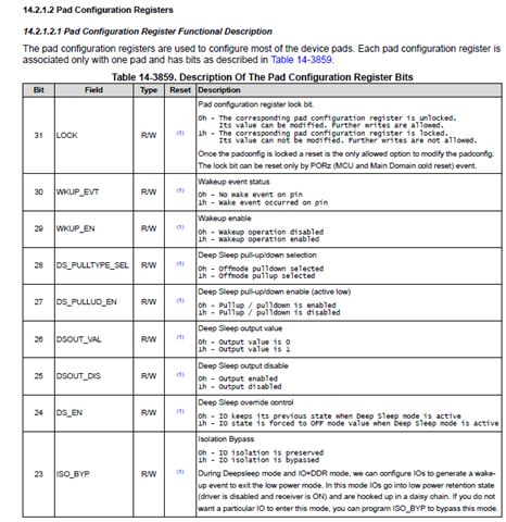
Pad configuration register lock bit. 0h - The corresponding pad configuration register is unlocked. Its value can be modified. Further writes are allowed. 1h - The corresponding pad configuration register is locked. Its value can not be modified. Further writes are not allowed. Once the padconfig is locked a reset is the only allowed option to modify the padconfig. The lock bit can be reset only by PORz (MCU and Main Domain cold reset) event. |
|
30-22 |
RESERVED |
Reserved |
|
21 |
TX_DIS(3) |
Driver Disable 0 - Driver is enabled 1 - Driver is disabled |
|
20 - 19 |
DRV_STR(4) |
Drive Strength Control. Selects the drive strength value for LVCMOS pins. (Does not apply to other pin types) |
|
18 |
RXACTIVE(5) |
Input enable for the Pad 0 - Receiver disabled 1 - Receiver enabled |
|
17 |
PULLTYPESEL |
Pad Pullup / Pulldown type selection 0 - Pulldown selected 1 - Pullup selected |
|
16 |
PULLUDEN(2) |
Pad Pullup / Pulldown enable. This is an active low signal. 0 - Pullup / Pulldown enabled 1 - Pullup / Pulldown disabled |
|
15 |
RESERVED |
Reserved |
|
14 |
ST_EN |
Receiver Schmitt Trigger enable 0 - Schmitt trigger input disabled 1 - Schmitt trigger input enabled |
|
13 - 11 |
DEBOUNCE_SEL |
Selects the debounce period for the pad. |
|
10 - 4 |
RESERVED |
Reserved |
|
3 - 0 |
MUXMODE |
Pad functional signal mux selection Field values (others are reserved) |
(1) See Pad Configuration Registers for reset values for Pad Configuration registers.
(2) These bits do not apply to "I2C OD FS" buffer types as these IOs do not have internal pull registers.
(3) To prevent unwanted glitches, software should disable the output driver by setting the TX_DIS bit before writing a new MUXMODE
value. Once the new MUXMODE value is written, the TX_DIS bit can be reset in order to re-enable the pin driver.
(4) Use of settings other than the reset value could invalidate datasheet timings.
Many of the device pads support pad multiplexing. This means that their function can be independently chosen
from two or more options. The selection of functions available on each pad is enumerated in table “Pin
Multiplexing” of the device-specific Datasheet. The desired function is selected via the MUXMODE field of the
associated pad configuration register.
PADCONFIG register additional input
(1) TX_DIS bit must be set before changing the MUXMODE value when the IO associated with a PADCONFIG register was previously configured to operate as an output. This is required
to prevent a potential glitch propagating through the output buffer when the MUXMODE values is changed. A MUXMODE value change should be implemented with three PADCONFIG
write operations, where the TX_DIS bit is set in the first write operation, the MUXMODE values is changed in the second write operation, and the TX_DIS bit is reset in the third write
operation. This will disable the output buffer while the pin mux logic changes signal functions.
(2) The RXACTIVE bit must never be set without a valid logic state being sourced to the pin associated with the respective PADCONFIG register. This is very important since a floating input
may damage the device.
AM64x and AM243x
TRM link: https://www.ti.com/lit/pdf/spruim2
TRM Revision: SPRUIM2H – MAY 2020 – REVISED OCTOBER 2023
5.1.1.4 Pad Configuration Registers
5.1.1.4.1 Pad Configuration Register Functional Description
Table 5-13. Description Of The Pad Configuration Register Bits
5.1.1.4.2 Pad Configuration Ball Names
Table 5-14. Pad Configuration Ball Names
Available GPIO instances
AM64x/AM243x
Signal Descriptions
GPIO
MAIN Domain Instances
GPIO0 Signal Descriptions
GPIO0_0 ... GPIO0_86
GPIO1 Signal Descriptions
GPIO1_0...GPIO1_79
MCU Domain Instances
MCU_GPIO0 Signal Descriptions
MCU_GPIO0_0...MCU_GPIO0_22
The PADCFG_CTRL0_CFG0_PADCONFIG0 to PADCFG_CTRL0_CFG0_PADCONFIG171 registers control the
signal multiplexing of modules in the device MAIN domain.
The PADCFG_CTRL0_CFG0_PADCONFIG0 to PADCFG_CTRL0_CFG0_PADCONFIG32 registers control the
signal multiplexing of modules in the device MCU domain.
Regards,
Sreenivasa
Hi Board Designers,
Input regarding PADCONFIG registers bits and TRM reference
Padconfig register bits and functions are different for Am62x and AM64x
Summary of the PADCONFIG register bits for AM62x (includes AM62A, AM62P, AM62L)
PADCONFIG register description section reference
14.2.1.2 Pad Configuration Registers
14.2.1.2.1 Pad Configuration Register Functional Description
Summary of the PADCONFIG register bits for AM62L
|
Bit |
Field |
Description (bit function name) |
|
31 |
LOCK |
Pad configuration register lock bit. 0h - The corresponding pad configuration register is unlocked. Its value can be modified. Further writes are allowed. 1h - The corresponding pad configuration register is locked. Its value can not be modified. Further writes are not allowed. Once the padconfig is locked a reset is the only allowed option to modify the padconfig. The lock bit can be reset only by PORz (MCU and Main Domain cold reset) event. |
|
30 |
WKUP_EVT |
Wakeup event status |
|
29 |
WKUP_EN |
Wakeup enable |
|
28 |
DS_PULLTYPE_SEL |
Deep Sleep pull-up/down selection |
|
27 |
DS_PULLUD_EN |
Deep Sleep pull-up/down enable (active low) |
|
26 |
DSOUT_VAL |
Deep Sleep output value |
|
25 |
DSOUT_DIS |
Deep Sleep output disable |
|
24 |
DS_EN |
Deep Sleep override control |
|
23 |
ISO_BYP |
Isolation Bypass |
|
22 |
RESERVED |
Reserved |
|
21 |
TX_DIS(3) |
Driver Disable 0 - Driver is enabled 1 - Driver is disabled |
|
20 - 19 |
DRV_STR(4) |
Drive Strength Control. Selects the drive strength value for LVCMOS pins. (Does not apply to other pin types) |
|
18 |
RXACTIVE(5) |
Input enable for the Pad 0 - Receiver disabled 1 - Receiver enabled |
|
17 |
PULLTYPESEL |
Pad Pullup / Pulldown type selection 0 - Pulldown selected 1 - Pullup selected |
|
16 |
PULLUDEN(2) |
Pad Pullup / Pulldown enable. This is an active low signal. 0 - Pullup / Pulldown enabled 1 - Pullup / Pulldown disabled |
|
15 |
FORCE_DS_EN |
Enable pad Deep Sleep controls by overriding DMSC gating |
|
14 |
ST_EN |
Receiver Schmitt Trigger enable 0 - Schmitt trigger input disabled 1 - Schmitt trigger input enabled |
|
13 - 11 |
DEBOUNCE_SEL |
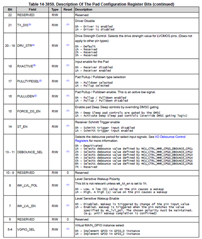
Selects the debounce period for select input signals. See I/O Debounce Control Registers for more information. |
|
10 - 9 |
RESERVED |
Reserved |
|
8 |
WK_LVL_POL |
Level Sensitive Wakeup Polarity |
|
7 |
WK_LVL_EN |
Level Sensitive Wakeup Enable |
|
6 |
RESERVED |
Reserved |
|
5-4 |
VGPIO_SEL |
Virtual MAIN_GPIO instance select |
|
3 - 0 |
MUXMODE |
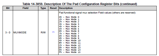
Pad functional signal mux selection Field values (others are reserved): |
Summary of the PADCONFIG register bits for AM62x, AM62A, AM62P
|
Bit |
Field |
Description (bit function name) |
|
31 |
LOCK |
Pad configuration register lock bit. 0h - The corresponding pad configuration register is unlocked. Its value can be modified. Further writes are allowed. 1h - The corresponding pad configuration register is locked. Its value can not be modified. Further writes are not allowed. Once the padconfig is locked a reset is the only allowed option to modify the padconfig. The lock bit can be reset only by PORz (MCU and Main Domain cold reset) event. |
|
30 |
WKUP_EVT |
Wakeup event status |
|
29 |
WKUP_EN |
Wakeup enable |
|
28 |
DS_PULLTYPE_SEL |
Deep Sleep pull-up/down selection |
|
27 |
DS_PULLUD_EN |
Deep Sleep pull-up/down enable (active low) |
|
26 |
DSOUT_VAL |
Deep Sleep output value |
|
25 |
DSOUT_DIS |
Deep Sleep output disable |
|
24 |
DS_EN |
Deep Sleep override control |
|
23 |
ISO_BYP |
Isolation Bypass |
|
22 |
RESERVED |
Reserved |
|
21 |
TX_DIS(3) |
Driver Disable 0 - Driver is enabled 1 - Driver is disabled |
|
20 - 19 |
DRV_STR(4) |
Drive Strength Control. Selects the drive strength value for LVCMOS pins. (Does not apply to other pin types) |
|
18 |
RXACTIVE(5) |
Input enable for the Pad 0 - Receiver disabled 1 - Receiver enabled |
|
17 |
PULLTYPESEL |
Pad Pullup / Pulldown type selection 0 - Pulldown selected 1 - Pullup selected |
|
16 |
PULLUDEN(2) |
Pad Pullup / Pulldown enable. This is an active low signal. 0 - Pullup / Pulldown enabled 1 - Pullup / Pulldown disabled |
|
15 |
FORCE_DS_EN |
Enable pad Deep Sleep controls by overriding DMSC gating |
|
14 |
ST_EN |
Receiver Schmitt Trigger enable 0 - Schmitt trigger input disabled 1 - Schmitt trigger input enabled |
|
13 - 11 |
DEBOUNCE_SEL |
Selects the debounce period for select input signals. See I/O Debounce Control Registers for more information. |
|
10 - 9 |
RESERVED |
Reserved |
|
8 |
WK_LVL_POL |
Level Sensitive Wakeup Polarity |
|
7 |
WK_LVL_EN |
Level Sensitive Wakeup Enable |
|
6-4 |
RESERVED |
Reserved |
|
3 - 0 |
MUXMODE |
Pad functional signal mux selection Field values (others are reserved): |
(1) See Pad Configuration Registers for reset values for Pad Configuration registers.
(2) These bits do not apply to "I2C OD FS" buffer types as these IOs do not have internal pull registers.
(3) To prevent unwanted glitches, software should disable the output driver by setting the TX_DIS bit before writing a new MUXMODE value. Once the new MUXMODE value is written, the TX_DIS bit can be reset in order to re-enable the pin driver.
(4) Use of settings other than the reset value could invalidate datasheet timings.
(5) The RXACTIVE bit must never be set without a valid logic state being sourced to the pin associated with the respective PADCONFIG register. This is very important since a floating input may damage the device.
Many of the device pads support pad multiplexing. This means that their function can be independently chosen from two or more options. The selection of functions available on each pad is enumerated in table “Pin Multiplexing” of the device-specific Datasheet. The desired function is selected via the MUXMODE field of the associated pad configuration register
PADCONFIG registers additional inputs
(1) TX_DIS bit must be set before changing the MUXMODE value when the IO associated with a PADCONFIG register was previously configured to operate as an output. This is required
to prevent a potential glitch propagating through the output buffer when the MUXMODE values is changed. A MUXMODE value change should be implemented with three PADCONFIG
write operations, where the TX_DIS bit is set in the first write operation, the MUXMODE values is changed in the second write operation, and the TX_DIS bit is reset in the third write
operation. This will disable the output buffer while the pin mux logic changes signal functions.
(2) Use of settings other than the reset value could invalidate datasheet timings.
(3) The RXACTIVE bit must never be set without a valid logic state being sourced to the pin associated with the respective PADCONFIG register. This is very important since a floating input
may damage the device.
(4) These bits do not apply to "I2C OD FS" buffer types as these IOs do not have internal pull registers.
(5) This PADCONFIG register is associated with a unbounded die pad that is used to insert timing compensation delays, where the MMC2 clock signal is looped through an output buffer and input buffer before being used to operate the MMCSD2 host controller. The RXACTIVE bit must be set and the TX_DIS bit must be reset before using MMC2. Note: the RXACTIVE
AM62x
TRM link: https://www.ti.com/lit/pdf/spruiv7
TRM Revision: SPRUIV7B – MAY 2022 – REVISED SEPTEMBER 2023
14.2.1.2 Pad Configuration Registers
14.2.1.2.1 Pad Configuration Register Functional Description
Table 14-6172. Description Of The Pad Configuration Register Bits
The table describes supported bit wise function for the 32-bit configuration register that can be referenced while configuring the PADCONFIG register for the specific functionality or use case (IO function)
14.2.1.2.2 Pad Configuration PADCONFIG Registers
The table below includes PADCONFIG Register Name & address, (includes padconfig registers that are not pinned out) and ball name (indicating one of the configurable function name) and default values for the 32 bits of all the supported PADCONFIG registers
Table 14-6173. Pad Configuration PADCONFIG Registers
Data sheet references
AM62x Sitara Processors datasheet (Rev. B)
https://www.ti.com/lit/pdf/sprsp58
Refer Pin Attributes and Signal Descriptions
GPIO
MAIN Domain
GPIO0 Signal Descriptions
GPIO0_0...GPIO0_91
GPIO1 Signal Descriptions
GPIO1_0...GPIO1_51
MCU Domain
MCU_GPIO0 Signal Descriptions
MCU_GPIO0_0...MCU_GPIO0_23
The PADCFG_CTRL0_CFG0_PADCONFIG0 to PADCFG_CTRL0_CFG0_PADCONFIG150 registers control the
signal multiplexing of modules in the device MAIN domain.
The PADCFG_CTRL0_CFG0_PADCONFIG0 to PADCFG_CTRL0_CFG0_PADCONFIG33 registers control the
signal multiplexing of modules in the device MCU domain.
AM62Ax/AM62Dx
Pad Configuration Registers related sections and tables available in TRM:
AM62Ax
TRM link: https://www.ti.com/lit/pdf/spruj16
TRM Revision: SPRUJ16B – DECEMBER 2021 – REVISED AUGUST 2023
14.2.1.2 Pad Configuration Registers
14.2.1.2.1 Pad Configuration Register Functional Description
Table 14-7176. Description Of The Pad Configuration Register Bits
14.2.1.2.2 Pad Configuration PADCONFIG Registers
Table 14-7177. Pad Configuration PADCONFIG Registers
AM62D-Q1
TRM link: https://www.ti.com/lit/pdf/sprujd4
TRM Revision: SPRUJD4 – DECEMBER 2024
14.2.1.2 Pad Configuration Registers
14.2.1.2.1 Pad Configuration Register Functional Description
Table 14-7402. Description Of The Pad Configuration Register Bits
14.2.1.2.2 Pad Configuration PADCONFIG Registers (Autogenerated)
Table 14-7403. AM62A PADCONFIG Registers
Signal Descriptions
GPIO
MAIN Domain Instances
GPIO0 Signal Descriptions
GPIO0_0...GPIO0_91
GPIO1 Signal Descriptions
GPIO1_0...GPIO1_51
MCU Domain Instances
MCU_GPIO0 Signal Descriptions
MCU_GPIO0_0...MCU_GPIO0_23
The PADCFG_CTRL0_CFG0_PADCONFIG0 to PADCFG_CTRL0_CFG0_PADCONFIG150 registers control the
signal multiplexing of modules in the device MAIN domain.
The PADCFG_CTRL0_CFG0_PADCONFIG0 to PADCFG_CTRL0_CFG0_PADCONFIG33 registers control the
signal multiplexing of modules in the device MCU domain.
AM62Px
TRM link: https://www.ti.com/lit/pdf/spruj83
TRM Revision: SPRUJ83B – DECEMBER 2023 – REVISED APRIL 2025
14.2.1.2 Pad Configuration Registers
14.2.1.2.1 Pad Configuration Register Functional Description
Table 14-8769. Description Of The Pad Configuration Register Bits
14.2.1.2.2 Pad Configuration PADCONFIG Registers (Autogenerated)
Table 14-8770. AM62P PADCONFIG Registers
AM62Px
Signal Descriptions
GPIO
MAIN Domain Instances
GPIO0 Signal Descriptions
GPIO0_0...GPIO0_91
GPIO1 Signal Descriptions
GPIO1_0...GPIO1_51
MCU Domain Instances
MCU_GPIO0 Signal Descriptions
MCU_GPIO0_0...MCU_GPIO0_23
The PADCFG_CTRL0_CFG0_PADCONFIG0 to PADCFG_CTRL0_CFG0_PADCONFIG150 registers control the
signal multiplexing of modules in the device MAIN domain.
The PADCFG_CTRL0_CFG0_PADCONFIG0 to PADCFG_CTRL0_CFG0_PADCONFIG33 registers control the
signal multiplexing of modules in the device MCU domain.
AM62L
TRM link: https://www.ti.com/lit/pdf/sprujb4
TRM Revision: SPRUJB4 – FEBRUARY 2025
14.2.1.2 Pad Configuration Registers
14.2.1.2.1 Pad Configuration Register Functional Description
Table 14-3859. Description Of The Pad Configuration Register Bits
14.2.1.2.2 Pad Configuration PADCONFIG Registers
Table 14-3860. Pad Configuration PADCONFIG Registers
Signal Descriptions
GPIO
MAIN Domain Instances
GPIO0 Signal Descriptions
GPIO0_0...GPIO0_99
WKUP Domain
WKUP_GPIO0 Signal Descriptions
WKUP_GPIO0_0...WKUP_GPIO0_6
The PADCFG_CTRL0_CFG0_PADCONFIG0 to PADCFG_CTRL0_CFG0_PADCONFIG146 registers control the
signal multiplexing of modules in the device MAIN domain.
Regards,
Sreenivasa