Part Number: AM6412
Tool/software:
Champ,
Is there QSPI timing specification for AM64x?
In Data Manual, there is only timing specification for McSPI and OSPI but not for QSPI.
BR, Rich
This thread has been locked.
If you have a related question, please click the "Ask a related question" button in the top right corner. The newly created question will be automatically linked to this question.
Hi Rich,
The OSPI timing requirements are valid also for QSPI chips. The point is, OSPI0 controller is supporting both OSPI and QSPI memories.
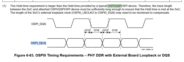
You can see in the OSPI section that the number of data pins is represented with variable 'i' and QSPI is sometimes mentioned :

I agree the section title may has to be adjusted.
Regards,
Stan
Stan,
Thanks for the explanation, we actually tried to use OSPI specification to check and take SDR mode specification.
The concern points here are the parameter setting in ROM code during QSPI booting.
We don't have the setting for M and N and R values so not sure the timing range expected.
May we have the setting during QSPI booting? Are these value default value in registers after reset?

BR, Rich
Rich,
ROM uses fail-safe timing settings so that majority of memories/interfaces on the market are covered. Therefore, I think M and N ROM code settings should not be a concern.
Below are other important conditions to meet (TRM section 4.4.1.3 QSPI Boot):
The QSPI boot mode supports the 1S-1S-4S mode only (Bit-width =1 or 4, Single Data Rate). The Command
and Address issued are 8 bits and 24 bits respectively. The Read Command that is issued for QSPI is 0x6b
followed by zero for address and 8 dummy cycles. The frequency of operation supported is 50 MHz.
Regards,
Stan
Stan,
Thanks for the information.
Do you mean ROM code will adjust the clock rate and timing for retry?
The concern point from field is the end customer would like to make sure the QSPI booting timing meets specification from SOC.
Therefore, they need to measure the waveforms and check if timing fall into required interval so they can confirm Signal Integrity is OK.
To ODM, they need exact the timing range (MAX or MIN) and compare with their actual measured waveform.
Without the M, N and R, we don't know the right timing range to follow.
Alternative, if team can provide the MIN and MAX value for O10 and O11 in ns.
In this case, ODM can get the criteria to check waveform.
BR, Rich
Rich,
I will check internally and come back as soon I have feedback.
Regards,
Stan
Hi Rich,
I'm still waiting for a response from the ROM team.
Regards,
Stan
Rich, I got the reply:
ROM code uses tap mode @ 50 MHz and not PHY mode.
In ROM, the DEV_DELAY_REG is set to 0x0.
What is actually used for tap mode is the RD_DATA_CAPTURE_REG DELAY_FLD bit[4:1]. For which we (ROM) scan all possible value to find the optimum setting.
So for ROM only DEV_DELAY_REG does not matter.
After boot, in their higher level s/w, if they would need/want to enable PHY mode to increase throughput then they would need to set these I imagined.
Regards,
Stan