Tool/software:
Hello Sir/Madam,
We are planning to migrate our platform based on AM335x Sitara family processor with part# AM3356BZCZA60 to the latest SDK. At the moment it is running on Linux Kernel (4.14.67), U-Boot (2018.01-00444-g96cdbef-dirty), and filesystem built using a Non-SDK variant of Yocto with SysV init system. Our intent is to migrate this what the latest SDK has to offer, skipping incremental SDK variants. As per the info on TI website https://www.ti.com/tool/PROCESSOR-SDK-AM335X#downloads, we see that the latest version is 09.03.05.02 release on Dec 13, 2024. On the Supported products & hardware sections it lists AM3356 which is the name of our SoC.
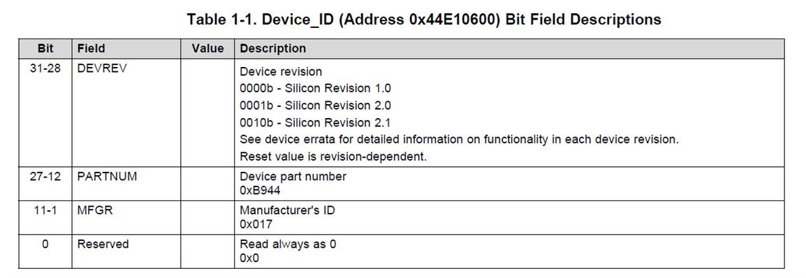
But since we are leapfrogging to a much higher version of the SDK with accompanying Kernel, U-Boot, Build tool chain, and Yocto distro; We wanted to check whether our hardware revision of the SoC will be fully supported by the components of this SDK. As per the part number and info printed on the chip and from the line "36CLGXW G1" we assume that the "G1" corresponds to Silicon Revision 1.0. Please correct us, if this interpretation is wrong!
We understand that with the latest SDKs may drop support for very old kernel/U-boot features or boot modes. They also might have errata which need to be applied/patched which may bring in some constraints. At the moment we are only considering the built-in devices/config of the SoC. External peripherals, and their specific driver/config need to be considered in the second stage.
Our current platform looks like this...
1GB DDR3
| ISSI | IS43TR16512B-125KBLI |
1GB NAND Flash
| MICRON | MT29F8G08ABACAH4-IT:C |
Attaching DTS for reference
So, our questions are...
- Although the support page mentions AM3356, it doesn't specifically mention about anything about hardware revisions. The latest SDK docs https://software-dl.ti.com/processor-sdk-linux/esd/docs/latest/linux/Release_Specific_Supported_Platforms_and_Versions.html#release-specific-supported-platforms-and-versions mentions EVMs, But again no direct mention of SoC revisions. Also the version on this page shows "07_03_00_005", not the 09.xx on the SDK download page.
- What is the recommended approach we should be taking for this upgrade? Will the SDK contain all the necessary patches, and guidance to apply those? The hardware and board design will not be changed.
- Can this be considered like a medium effort upgrade (only till the SoC is up, not including external peripherals), or will it be tall order?
- Are there any other factors we need to be considering?
/*
 * Copyright (C) 2012 Texas Instruments Incorporated - http://www.ti.com/
 *
 * This program is free software; you can redistribute it and/or modify
 * it under the terms of the GNU General Public License version 2 as
 * published by the Free Software Foundation.
 */
/dts-v1/;

#include "am33xx.dtsi"
#include <dt-bindings/interrupt-controller/irq.h>
#include <dt-bindings/net/ti-dp83869.h>

/ {
	model = "SYNC 2000-M5";
	compatible = "ti,am335x-evm", "ti,am33xx";

	cpus {
		cpu@0 {
			cpu0-supply = <&vdd1_reg>;
		};
	};

	memory@80000000 {
		device_type = "memory";
		reg = <0x80000000 0x10000000>; /* 256 MB */
	};

	vbat: fixedregulator0 {
		compatible = "regulator-fixed";
		regulator-name = "vbat";
		regulator-min-microvolt = <5000000>;
		regulator-max-microvolt = <5000000>;
		regulator-boot-on;
	};

	lis3_reg: fixedregulator1 {
		compatible = "regulator-fixed";
		regulator-name = "lis3_reg";
		regulator-boot-on;
	};

};

&am33xx_pinmux {
	pinctrl-names = "default";

	pinctrl-0 = <&gpio0_pins &gpio1_pins &gpio2_pins &gpio3_pins>;

	gpio0_pins: pinmux_gpio0_pins {
		pinctrl-single,pins = <
			0x2C (PIN_OUTPUT | MUX_MODE7) /* gpio0_27 *//*Com2 uart0 232 enable*/
			0x28 (PIN_OUTPUT | MUX_MODE7) /* GPIO0_26 watchdog pulse */

		>;
	};

	gpio1_pins: pinmux_gpio1_pins {
		pinctrl-single,pins = <
			0x30  (PIN_OUTPUT | MUX_MODE7) /* gpio1_12 *//*Com3 uart3 232 enable*/ /* STR */
			0x34  (PIN_OUTPUT_PULLUP | MUX_MODE7) /* gpio1_13 */ /*Com4 uart5 232 enable*/ /* STR */
			0x78  (PIN_OUTPUT | MUX_MODE7) /* gpio1_28,conf_gpmc_ben1,DO_buffer enable */
			0x84  (PIN_INPUT | MUX_MODE7) /* gpio1_31,conf_gpmc_csn2 */ /*gprs power shutdown */
		>;
	};

	gpio2_pins: pinmux_gpio2_pins {
		pinctrl-single,pins = <
			0x8C  (PIN_INPUT_PULLUP | MUX_MODE7)    /* gpio2_1 usb over current from external source*/
			0xE4  (PIN_OUTPUT | MUX_MODE7) /* gpio2_23 */  /* STR */
			0xEC  (PIN_OUTPUT_PULLUP | MUX_MODE7) 	/* GPIO2_25 ,conf_lcd_ac_bias_en,health status */
		>;
	};

	gpio3_pins: pinmux_gpio3_pins {
		pinctrl-single,pins = <
			0x1A0  (PIN_OUTPUT | MUX_MODE7) /* gpio3_18 */
			/*0x1A8  (PIN_OUTPUT | MUX_MODE7)*/ /* gpio3_20,conf_mcasp0 */ /*gprs hard shutdown */
			0x234  (PIN_OUTPUT_PULLUP | MUX_MODE7) /* gpio3_13,conf_usb1_drvvbu,DO_Buff */
			0x1A0  (PIN_OUTPUT | MUX_MODE7) /* GPIO3_18,conf_mcasp0_aclkr,profibus */
			0x198  (PIN_OUTPUT  | MUX_MODE7) /* GPIO3_16,conf_mcasp0_axr0,debug */
		>;
	};

	i2c0_pins: pinmux_i2c0_pins {
		pinctrl-single,pins = <
			AM33XX_IOPAD(0x988, PIN_INPUT_PULLUP | MUX_MODE0)	/* i2c0_sda.i2c0_sda */
			AM33XX_IOPAD(0x98c, PIN_INPUT_PULLUP | MUX_MODE0)	/* i2c0_scl.i2c0_scl */
		>;
	};

	i2c1_pins: pinmux_i2c1_pins {
		pinctrl-single,pins = <
			AM33XX_IOPAD(0x958, PIN_INPUT_PULLUP | MUX_MODE2)	/* spi0_d1.i2c1_sda */
			AM33XX_IOPAD(0x95c, PIN_INPUT_PULLUP | MUX_MODE2)	/* spi0_cs0.i2c1_scl */
		>;
	};

	i2c2_pins: pinmux_i2c2_pins {
			pinctrl-single,pins = <
				0x150 (PIN_INPUT_PULLUP | MUX_MODE2)	/* spi0_sclk.i2c0_sda */
				0x154 (PIN_INPUT_PULLUP | MUX_MODE2)	/* spi0_d0.i2c0_scl */
			>;
		};
	spi1_pins: pinmux_spi1_pins {       			/*MAX14830 SPI-Quad-UART*/
		pinctrl-single,pins = <
			0x1A8  (PIN_OUTPUT_PULLUP | MUX_MODE7) /* gpio3_20,conf_mcasp0 */ /*QUART_RST PIN, Previosuly gprs shutdown pin */
			/*0x84  (PIN_OUTPUT_PULLUP | MUX_MODE7)*/  /* gpio1_31,conf_gpmc_csn2 */ /*gprs power shutdown, IRQ */
			0x108 (PIN_INPUT_PULLUP | MUX_MODE2) /* clock */
			0x110 (PIN_INPUT_PULLUP | MUX_MODE2) /* MISO, D1 */
			0x10C (PIN_OUTPUT_PULLUP | MUX_MODE2)	/* MOSI ,D0 */
			0x144 (PIN_OUTPUT_PULLUP | MUX_MODE7)	/*CS0*/
		>;
	};
	uart0_pins: pinmux_uart0_pins {
		pinctrl-single,pins = <
			0x168 (PIN_INPUT | MUX_MODE0)		/* uart0_ctsn.uart0_ctsn */
			0x16C (PIN_OUTPUT_PULLDOWN | MUX_MODE7)	/* uart0_rtsn .uart0_rtsn  */
			0x170 (PIN_INPUT_PULLUP | MUX_MODE0)	/* uart0_rxd.uart0_rxd */
			0x174 (PIN_OUTPUT_PULLDOWN | MUX_MODE0)	/* uart0_txd.uart0_txd */
		>;
	};
	uart1_pins: pinmux_uart1_pins {
		pinctrl-single,pins = <
			0x178 (PIN_INPUT | MUX_MODE0)		/* uart1_ctsn.uart1_ctsn */
			0x17C (PIN_OUTPUT_PULLDOWN | MUX_MODE0)	/* uart1_rtsn.uart1_rtsn */
			0x180 (PIN_INPUT_PULLUP | MUX_MODE0)	/* uart1_rxd.uart1_rxd */
			0x184 (PIN_OUTPUT_PULLDOWN | MUX_MODE0)	/* uart1_txd.uart1_txd */
			0xFC (PIN_INPUT | MUX_MODE4)		/* mmc0_dat0.uart1_ri */
			0xF8 (PIN_OUTPUT_PULLDOWN | MUX_MODE4)	/* mmc0_dat0.uart1_dtr */
			0xF4 (PIN_INPUT | MUX_MODE4)		/* mmc0_dat0.uart1_dsr */
			0xF0 (PIN_INPUT | MUX_MODE4)		/* mmc0_dat0.uart1_dcd */
		>;
	};

	uart3_pins: pinmux_uart3_pins {
		pinctrl-single,pins = <
			0x164 (PIN_OUTPUT_PULLDOWN | MUX_MODE1)	/* ecap0_in_pwm0_out.UART3_TXD */
			0x160 (PIN_INPUT_PULLUP | MUX_MODE1)	/* spi0_cs1.UART3_RXD */
			0xCC (PIN_OUTPUT_PULLDOWN | MUX_MODE7)	/* LCD_DATA11.UART3_RTSN */
			0xC8 (PIN_INPUT | MUX_MODE6)		/* LCD_DATA10.UART3_CTSN */
		>;
	};
	uart5_pins: pinmux_uart5_pins {
		pinctrl-single,pins = <
			0xD8 (PIN_INPUT | MUX_MODE6)		/* lcd_data14.uart5_ctsn */
			0xC4 (PIN_INPUT_PULLUP | MUX_MODE4)	/* lcd_data9.uart5_rxd */
			0xC0 (PIN_OUTPUT_PULLDOWN | MUX_MODE4)  /* lcd_data8.uart5_txd */
			0xDC (PIN_OUTPUT_PULLDOWN | MUX_MODE7)	/* lcd_data15.uart5_rtsn */
		>;
	};

	nandflash_pins_s0: nandflash_pins_s0 {
		pinctrl-single,pins = <
			AM33XX_IOPAD(0x800, PIN_INPUT_PULLUP | MUX_MODE0)	/* gpmc_ad0.gpmc_ad0 */
			AM33XX_IOPAD(0x804, PIN_INPUT_PULLUP | MUX_MODE0)	/* gpmc_ad1.gpmc_ad1 */
			AM33XX_IOPAD(0x808, PIN_INPUT_PULLUP | MUX_MODE0)	/* gpmc_ad2.gpmc_ad2 */
			AM33XX_IOPAD(0x80c, PIN_INPUT_PULLUP | MUX_MODE0)	/* gpmc_ad3.gpmc_ad3 */
			AM33XX_IOPAD(0x810, PIN_INPUT_PULLUP | MUX_MODE0)	/* gpmc_ad4.gpmc_ad4 */
			AM33XX_IOPAD(0x814, PIN_INPUT_PULLUP | MUX_MODE0)	/* gpmc_ad5.gpmc_ad5 */
			AM33XX_IOPAD(0x818, PIN_INPUT_PULLUP | MUX_MODE0)	/* gpmc_ad6.gpmc_ad6 */
			AM33XX_IOPAD(0x81c, PIN_INPUT_PULLUP | MUX_MODE0)	/* gpmc_ad7.gpmc_ad7 */
			AM33XX_IOPAD(0x870, PIN_INPUT_PULLUP | MUX_MODE0)	/* gpmc_wait0.gpmc_wait0 */
			AM33XX_IOPAD(0x874, PIN_INPUT_PULLUP | MUX_MODE7)	/* gpmc_wpn.gpio0_30 */
			AM33XX_IOPAD(0x87c, PIN_OUTPUT | MUX_MODE0)		/* gpmc_csn0.gpmc_csn0  */
			AM33XX_IOPAD(0x890, PIN_OUTPUT | MUX_MODE0)		/* gpmc_advn_ale.gpmc_advn_ale */
			AM33XX_IOPAD(0x894, PIN_OUTPUT | MUX_MODE0)		/* gpmc_oen_ren.gpmc_oen_ren */
			AM33XX_IOPAD(0x898, PIN_OUTPUT | MUX_MODE0)		/* gpmc_wen.gpmc_wen */
			AM33XX_IOPAD(0x89c, PIN_OUTPUT | MUX_MODE0)		/* gpmc_be0n_cle.gpmc_be0n_cle */
		>;
	};

	ecap0_pins: backlight_pins {
		pinctrl-single,pins = <
			AM33XX_IOPAD(0x964, MUX_MODE0)	/* eCAP0_in_PWM0_out.eCAP0_in_PWM0_out */
		>;
	};

	cpsw_default: cpsw_default {
		pinctrl-single,pins = <
			/* Slave 1 */
			0x114 (PIN_OUTPUT_PULLDOWN | MUX_MODE2)	/* mii1_txen.rgmii1_tctl */
			0x118 (PIN_INPUT_PULLDOWN | MUX_MODE2)	/* mii1_rxdv.rgmii1_rctl */
			0x11c (PIN_OUTPUT_PULLDOWN | MUX_MODE2)	/* mii1_txd3.rgmii1_td3 */
			0x120 (PIN_OUTPUT_PULLDOWN | MUX_MODE2)	/* mii1_txd2.rgmii1_td2 */
			0x124 (PIN_OUTPUT_PULLDOWN | MUX_MODE2)	/* mii1_txd1.rgmii1_td1 */
			0x128 (PIN_OUTPUT_PULLDOWN | MUX_MODE2)	/* mii1_txd0.rgmii1_td0 */
			0x12c (PIN_OUTPUT_PULLDOWN | MUX_MODE2)	/* mii1_txclk.rgmii1_tclk */
			0x130 (PIN_INPUT_PULLDOWN | MUX_MODE2)	/* mii1_rxclk.rgmii1_rclk */
			0x134 (PIN_INPUT_PULLDOWN | MUX_MODE2)	/* mii1_rxd3.rgmii1_rd3 */
			0x138 (PIN_INPUT_PULLDOWN | MUX_MODE2)	/* mii1_rxd2.rgmii1_rd2 */
			0x13c (PIN_INPUT_PULLDOWN | MUX_MODE2)	/* mii1_rxd1.rgmii1_rd1 */
			0x140 (PIN_INPUT_PULLDOWN | MUX_MODE2)	/* mii1_rxd0.rgmii1_rd0 */

			/* Slave 2 */
			0x40 (PIN_OUTPUT_PULLDOWN | MUX_MODE2)	/* gpmc_a0.rgmii2_tctl */
			0x44 (PIN_INPUT_PULLDOWN | MUX_MODE2)	/* gpmc_a1.rgmii2_rctl */
			0x48 (PIN_OUTPUT_PULLDOWN | MUX_MODE2)	/* gpmc_a2.rgmii2_td3 */
			0x4c (PIN_OUTPUT_PULLDOWN | MUX_MODE2)	/* gpmc_a3.rgmii2_td2 */
			0x50 (PIN_OUTPUT_PULLDOWN | MUX_MODE2)	/* gpmc_a4.rgmii2_td1 */
			0x54 (PIN_OUTPUT_PULLDOWN | MUX_MODE2)	/* gpmc_a5.rgmii2_td0 */
			0x58 (PIN_OUTPUT_PULLDOWN | MUX_MODE2)	/* gpmc_a6.rgmii2_tclk */
			0x5c (PIN_INPUT_PULLDOWN | MUX_MODE2)	/* gpmc_a7.rgmii2_rclk */
			0x60 (PIN_INPUT_PULLDOWN | MUX_MODE2)	/* gpmc_a8.rgmii2_rd3 */
			0x64 (PIN_INPUT_PULLDOWN | MUX_MODE2)	/* gpmc_a9.rgmii2_rd2 */
			0x68 (PIN_INPUT_PULLDOWN | MUX_MODE2)	/* gpmc_a10.rgmii2_rd1 */
			0x6c (PIN_INPUT_PULLDOWN | MUX_MODE2)	/* gpmc_a11.rgmii2_rd0 */
		>;
	};

	cpsw_sleep: cpsw_sleep {
		pinctrl-single,pins = <
			/* Slave 1 reset value */
			0x114 (PIN_INPUT_PULLDOWN | MUX_MODE7)
			0x118 (PIN_INPUT_PULLDOWN | MUX_MODE7)
			0x11c (PIN_INPUT_PULLDOWN | MUX_MODE7)
			0x120 (PIN_INPUT_PULLDOWN | MUX_MODE7)
			0x124 (PIN_INPUT_PULLDOWN | MUX_MODE7)
			0x128 (PIN_INPUT_PULLDOWN | MUX_MODE7)
			0x12c (PIN_INPUT_PULLDOWN | MUX_MODE7)
			0x130 (PIN_INPUT_PULLDOWN | MUX_MODE7)
			0x134 (PIN_INPUT_PULLDOWN | MUX_MODE7)
			0x138 (PIN_INPUT_PULLDOWN | MUX_MODE7)
			0x13c (PIN_INPUT_PULLDOWN | MUX_MODE7)
			0x140 (PIN_INPUT_PULLDOWN | MUX_MODE7)

			/* Slave 2 reset value*/
			0x40 (PIN_INPUT_PULLDOWN | MUX_MODE7)
			0x44 (PIN_INPUT_PULLDOWN | MUX_MODE7)
			0x48 (PIN_INPUT_PULLDOWN | MUX_MODE7)
			0x4c (PIN_INPUT_PULLDOWN | MUX_MODE7)
			0x50 (PIN_INPUT_PULLDOWN | MUX_MODE7)
			0x54 (PIN_INPUT_PULLDOWN | MUX_MODE7)
			0x58 (PIN_INPUT_PULLDOWN | MUX_MODE7)
			0x5c (PIN_INPUT_PULLDOWN | MUX_MODE7)
			0x60 (PIN_INPUT_PULLDOWN | MUX_MODE7)
			0x64 (PIN_INPUT_PULLDOWN | MUX_MODE7)
			0x68 (PIN_INPUT_PULLDOWN | MUX_MODE7)
			0x6c (PIN_INPUT_PULLDOWN | MUX_MODE7)
		>;
	};

	davinci_mdio_default: davinci_mdio_default {
		pinctrl-single,pins = <
			/* MDIO */
			AM33XX_IOPAD(0x948, PIN_INPUT_PULLUP | SLEWCTRL_FAST | MUX_MODE0)	/* mdio_data.mdio_data */
			AM33XX_IOPAD(0x94c, PIN_OUTPUT_PULLUP | MUX_MODE0)			/* mdio_clk.mdio_clk */
		>;
	};

	davinci_mdio_sleep: davinci_mdio_sleep {
		pinctrl-single,pins = <
			/* MDIO reset value */
			AM33XX_IOPAD(0x948, PIN_INPUT_PULLDOWN | MUX_MODE7)
			AM33XX_IOPAD(0x94c, PIN_INPUT_PULLDOWN | MUX_MODE7)
		>;
	};

	mmc1_pins: pinmux_mmc1_pins {
		pinctrl-single,pins = <
			AM33XX_IOPAD(0x960, PIN_INPUT | MUX_MODE7)		/* spi0_cs1.gpio0_6 */
			AM33XX_IOPAD(0x8fc, PIN_INPUT_PULLUP | MUX_MODE0)	/* mmc0_dat0.mmc0_dat0 */
			AM33XX_IOPAD(0x8f8, PIN_INPUT_PULLUP | MUX_MODE0)	/* mmc0_dat1.mmc0_dat1 */
			AM33XX_IOPAD(0x8f4, PIN_INPUT_PULLUP | MUX_MODE0)	/* mmc0_dat2.mmc0_dat2 */
			AM33XX_IOPAD(0x8f0, PIN_INPUT_PULLUP | MUX_MODE0)	/* mmc0_dat3.mmc0_dat3 */
			AM33XX_IOPAD(0x904, PIN_INPUT_PULLUP | MUX_MODE0)	/* mmc0_cmd.mmc0_cmd */
			AM33XX_IOPAD(0x900, PIN_INPUT_PULLUP | MUX_MODE0)	/* mmc0_clk.mmc0_clk */
			AM33XX_IOPAD(0x9a0, PIN_INPUT | MUX_MODE4)		/* mcasp0_aclkr.mmc0_sdwp */
		>;
	};

	mmc3_pins: pinmux_mmc3_pins {
		pinctrl-single,pins = <
			AM33XX_IOPAD(0x844, PIN_INPUT_PULLUP | MUX_MODE3)	/* gpmc_a1.mmc2_dat0, INPUT_PULLUP | MODE3 */
			AM33XX_IOPAD(0x848, PIN_INPUT_PULLUP | MUX_MODE3)	/* gpmc_a2.mmc2_dat1, INPUT_PULLUP | MODE3 */
			AM33XX_IOPAD(0x84c, PIN_INPUT_PULLUP | MUX_MODE3)	/* gpmc_a3.mmc2_dat2, INPUT_PULLUP | MODE3 */
			AM33XX_IOPAD(0x878, PIN_INPUT_PULLUP | MUX_MODE3)	/* gpmc_ben1.mmc2_dat3, INPUT_PULLUP | MODE3 */
			AM33XX_IOPAD(0x888, PIN_INPUT_PULLUP | MUX_MODE3)	/* gpmc_csn3.mmc2_cmd, INPUT_PULLUP | MODE3 */
			AM33XX_IOPAD(0x88c, PIN_INPUT_PULLUP | MUX_MODE3)	/* gpmc_clk.mmc2_clk, INPUT_PULLUP | MODE3 */
		>;
	};

	mcasp1_pins: mcasp1_pins {
		pinctrl-single,pins = <
			AM33XX_IOPAD(0x90c, PIN_INPUT_PULLDOWN | MUX_MODE4) /* mii1_crs.mcasp1_aclkx */
			AM33XX_IOPAD(0x910, PIN_INPUT_PULLDOWN | MUX_MODE4) /* mii1_rxerr.mcasp1_fsx */
			AM33XX_IOPAD(0x908, PIN_OUTPUT_PULLDOWN | MUX_MODE4) /* mii1_col.mcasp1_axr2 */
			AM33XX_IOPAD(0x944, PIN_INPUT_PULLDOWN | MUX_MODE4) /* rmii1_ref_clk.mcasp1_axr3 */
		>;
	};

	mcasp1_pins_sleep: mcasp1_pins_sleep {
		pinctrl-single,pins = <
			AM33XX_IOPAD(0x90c, PIN_INPUT_PULLDOWN | MUX_MODE7)
			AM33XX_IOPAD(0x910, PIN_INPUT_PULLDOWN | MUX_MODE7)
			AM33XX_IOPAD(0x908, PIN_INPUT_PULLDOWN | MUX_MODE7)
			AM33XX_IOPAD(0x944, PIN_INPUT_PULLDOWN | MUX_MODE7)
		>;
	};

	dcan1_pins_default: dcan1_pins_default {
		pinctrl-single,pins = <
			AM33XX_IOPAD(0x968, PIN_OUTPUT | MUX_MODE2) /* uart0_ctsn.d_can1_tx */
			AM33XX_IOPAD(0x96c, PIN_INPUT_PULLDOWN | MUX_MODE2) /* uart0_rtsn.d_can1_rx */
		>;
	};

};

&usb {
	status = "okay";
};

&usb_ctrl_mod {
	status = "okay";
};

&usb0_phy {
	status = "okay";
};

&usb1_phy {
	status = "okay";
};

&usb0 {
	status = "okay";
	dr_mode = "host";
};

&usb1 {
	status = "okay";
	disable-over-current;
};

&cppi41dma  {
        status = "okay";
};

&spi1 {
	pinctrl-names = "default";
	pinctrl-0 = <&spi1_pins>;
	status = "okay";
    	cs-gpios = <&gpio0 29 GPIO_ACTIVE_LOW>;
    	num-cs = <1>;
	ti,pindir-d0-out-d1-in;

	max14830: max14830@0 {   /* Midhun */
				compatible = "maxim,max14830";
				reg = <0>;
				spi-max-frequency = <5000000>;
				clocks = <&clk24m0>;
				clock-names = "xtal"; /* Midhun */
				interrupt-parent = <&gpio1>;
				interrupts = <31 IRQ_TYPE_EDGE_FALLING>;
				gpio-controller;
				#gpio-cells = <2>;
				clk24m0: clk24m0 {
				compatible = "fixed-clock";
				#clock-cells = <0>;
				clock-frequency = <3686400>;
				clock-accuracy = <100>;
				};
			};
};

&uart0 {
	pinctrl-names = "default";
	pinctrl-0 = <&uart0_pins>;
	status = "okay";
	rts-gpio = <&gpio1 9 GPIO_ACTIVE_HIGH>;
	rs485-rts-active-high;
	rs485-rts-delay = <2 1>;
	linux,rs485-enabled-at-boot-time;
};

&uart1 {
	pinctrl-names = "default";
	pinctrl-0 = <&uart1_pins>;
	status = "okay";
};

&uart3 {
	pinctrl-names = "default";
	pinctrl-0 = <&uart3_pins>;
	status = "okay";
	rts-gpio = <&gpio2 17 GPIO_ACTIVE_HIGH>;
	rs485-rts-active-high;
	rs485-rts-delay = <2 1>;
	linux,rs485-enabled-at-boot-time;
};

&uart5 {
	pinctrl-names = "default";
	pinctrl-0 = <&uart5_pins>;
	status = "okay";
	rts-gpio = <&gpio0 11 GPIO_ACTIVE_HIGH>;
	rs485-rts-active-high;
	rs485-rts-delay = <2 1>;
	linux,rs485-enabled-at-boot-time;
};

&i2c0 {
	pinctrl-names = "default";
	pinctrl-0 = <&i2c0_pins>;

	status = "okay";
	clock-frequency = <400000>;

	/* Set OPP50 (0.95V) for VDD core */
	sleep-sequence = /bits/ 8 <
		0x02 0x2d 0x25 0x1f /* Set VDD2 to 0.95V */
	>;

	/* Set OPP100 (1.10V) for VDD core */
	wake-sequence = /bits/ 8 <
		0x02 0x2d 0x25 0x2b /* Set VDD2 to 1.1V */
	>;

	tps: tps@2d {
		reg = <0x2d>;
	};
	rtc@68 {
		compatible = "dallas,ds1388";
		reg = <0x68>;
	};
};

&i2c1 {
	pinctrl-names = "default";
	pinctrl-0 = <&i2c1_pins>;

	status = "okay";
	clock-frequency = <100000>;

	/* Set OPP50 (0.95V) for VDD core */
	sleep-sequence = /bits/ 8 <
		0x02 0x2d 0x25 0x1f /* Set VDD2 to 0.95V */
	>;

	/* Set OPP100 (1.10V) for VDD core */
	wake-sequence = /bits/ 8 <
		0x02 0x2d 0x25 0x2b /* Set VDD2 to 1.1V */
	>;
};

&i2c2 {
	status = "okay";
	pinctrl-names = "default";
	pinctrl-0 = <&i2c2_pins>;
};

&gpio0 {
	/*ti,no-reset-on-init;*/
	status = "okay";
	pinctrl-names = "default";
};
&gpio1 {

	ti,no-reset-on-init;
	status = "okay";
	pinctrl-names = "default";
};

&gpio2 {
	ti,no-reset-on-init;
	status = "okay";
	pinctrl-names = "default";
};

&gpio3 {
	status = "okay";
	pinctrl-names = "default";
	ti,no-reset-on-init;
};

&elm {
	status = "okay";
};

&gpmc {
	status = "okay";
	pinctrl-names = "default";
	pinctrl-0 = <&nandflash_pins_s0>;
	ranges = <0 0 0x08000000 0x1000000>;	/* CS0: 16MB for NAND */
	nand@0,0 {
		compatible = "ti,omap2-nand";
		reg = <0 0 4>; /* CS0, offset 0, IO size 4 */
		interrupt-parent = <&gpmc>;
		interrupts = <0 IRQ_TYPE_NONE>, /* fifoevent */
			     <1 IRQ_TYPE_NONE>;	/* termcount */
		rb-gpios = <&gpmc 0 GPIO_ACTIVE_HIGH>; /* gpmc_wait0 */
		ti,nand-xfer-type = "prefetch-dma";
		ti,nand-ecc-opt = "bch16";
		ti,elm-id = <&elm>;
		nand-bus-width = <8>;
		gpmc,device-width = <1>;
		gpmc,sync-clk-ps = <0>;
		gpmc,cs-on-ns = <0>;
		gpmc,cs-rd-off-ns = <44>;
		gpmc,cs-wr-off-ns = <44>;
		gpmc,adv-on-ns = <6>;
		gpmc,adv-rd-off-ns = <34>;
		gpmc,adv-wr-off-ns = <44>;
		gpmc,we-on-ns = <0>;
		gpmc,we-off-ns = <40>;
		gpmc,oe-on-ns = <0>;
		gpmc,oe-off-ns = <54>;
		gpmc,access-ns = <64>;
		gpmc,rd-cycle-ns = <82>;
		gpmc,wr-cycle-ns = <82>;
		gpmc,bus-turnaround-ns = <0>;
		gpmc,cycle2cycle-delay-ns = <0>;
		gpmc,clk-activation-ns = <0>;
		gpmc,wr-access-ns = <40>;
		gpmc,wr-data-mux-bus-ns = <0>;
		/* MTD partition table */
		/* All SPL-* partitions are sized to minimal length
		 * which can be independently programmable. For
		 * NAND flash this is equal to size of erase-block */
		#address-cells = <1>;
		#size-cells = <1>;
		partition@0 {
			label = "NAND.SPL";
			reg = <0x00000000 0x00040000>;
		};
		partition@1 {
			label = "NAND.SPL.backup1";
			reg = <0x00040000 0x00040000>;
		};
		partition@2 {
			label = "NAND.SPL.backup2";
			reg = <0x00080000 0x00040000>;
		};
		partition@3 {
			label = "NAND.SPL.backup3";
			reg = <0x000C0000 0x00040000>;
		};
		partition@4 {
			label = "NAND.u-boot";
			reg = <0x00100000 0x00200000>;
		};
		partition@5 {
			label = "NAND.u-boot-env1";
			reg = <0x00300000 0x00040000>;
		};
		partition@6 {
			label = "NAND.u-boot-env2";
			reg = <0x00340000 0x00040000>;
		};
		partition@7 {
			label = "NAND.RBlob";
			reg = <0x00380000 0x03FC80000>;
		};
	};
};

#include "tps65910.dtsi"

&tps {
	vcc1-supply = <&vbat>;
	vcc2-supply = <&vbat>;
	vcc3-supply = <&vbat>;
	vcc4-supply = <&vbat>;
	vcc5-supply = <&vbat>;
	vcc6-supply = <&vbat>;
	vcc7-supply = <&vbat>;
	vccio-supply = <&vbat>;

	regulators {

		vrtc_reg: regulator@0 {

			regulator-always-on;
		};

		vio_reg: regulator@1 {
			regulator-always-on;
		};

		vdd1_reg: regulator@2 {
			/* VDD_MPU voltage limits 0.95V - 1.26V with +/-4% tolerance */
			regulator-name = "vdd_mpu";
			regulator-min-microvolt = <912500>;
			regulator-max-microvolt = <1351500>;
			regulator-boot-on;
			regulator-always-on;
		};

		vdd2_reg: regulator@3 {
			/* VDD_CORE voltage limits 0.95V - 1.1V with +/-4% tolerance */
			regulator-name = "vdd_core";
			regulator-min-microvolt = <912500>;
			regulator-max-microvolt = <1150000>;
			regulator-boot-on;
			regulator-always-on;
		};

		vdd3_reg: regulator@4 {
			regulator-always-on;
		};

		vdig1_reg: regulator@5 {
			regulator-always-on;
		};

		vdig2_reg: regulator@6 {
			regulator-always-on;
		};

		vpll_reg: regulator@7 {
			regulator-always-on;
		};

		vdac_reg: regulator@8 {
			regulator-always-on;
		};

		vaux1_reg: regulator@9 {
			regulator-always-on;
		};

		vaux2_reg: regulator@10 {
			regulator-always-on;
		};

		vaux33_reg: regulator@11 {
			regulator-always-on;
		};

		vmmc_reg: regulator@12 {
			regulator-min-microvolt = <1800000>;
			regulator-max-microvolt = <3300000>;
			regulator-always-on;
		};
	};
};

&mac {
	pinctrl-names = "default", "sleep";
	pinctrl-0 = <&cpsw_default>;
	pinctrl-1 = <&cpsw_sleep>;
	dual_emac = <2>;
	status = "okay";
};

&davinci_mdio {
	pinctrl-names = "default", "sleep";
	pinctrl-0 = <&davinci_mdio_default>;
	pinctrl-1 = <&davinci_mdio_sleep>;
	status = "okay";

	dp83869_0: ethernet-phy@2 {
		reg = <2>;
		tx-fifo-depth = <DP83869_PHYCR_FIFO_DEPTH_4_B_NIB>;
		rx-fifo-depth = <DP83869_PHYCR_FIFO_DEPTH_4_B_NIB>;
		ti,op-mode = <DP83869_RGMII_100_BASE>;
		ti,max-output-impedance = "true";
		ti,clk-output-sel = <DP83869_CLK_O_SEL_CHN_A_RCLK>;
		rx-internal-delay-ps = <2000>;
		tx-internal-delay-ps = <2000>;
	};

	dp83869_1: ethernet-phy@3 {
		reg = <3>;
		tx-fifo-depth = <DP83869_PHYCR_FIFO_DEPTH_4_B_NIB>;
		rx-fifo-depth = <DP83869_PHYCR_FIFO_DEPTH_4_B_NIB>;
		ti,op-mode = <DP83869_RGMII_100_BASE>;
		ti,max-output-impedance = "true";
		ti,clk-output-sel = <DP83869_CLK_O_SEL_CHN_A_RCLK>;
		rx-internal-delay-ps = <2000>;
		tx-internal-delay-ps = <2000>;
	};
};

&cpsw_emac0 {
	phy_id = <&davinci_mdio>, <2>;
	phy-mode = "rgmii-txid";
	dual_emac_res_vlan = <1>;
};

&cpsw_emac1 {
	phy_id = <&davinci_mdio>, <3>;
	phy-mode = "rgmii-txid";
	dual_emac_res_vlan = <2>;
};

&dcan1 {
	status = "disabled";	/* Enable only if Profile 1 is selected */
	pinctrl-names = "default";
	pinctrl-0 = <&dcan1_pins_default>;
};