


Other Parts Discussed in Thread: DP83869
Tool/software:
Hi Team,
SDK version using :
09.02.00.05
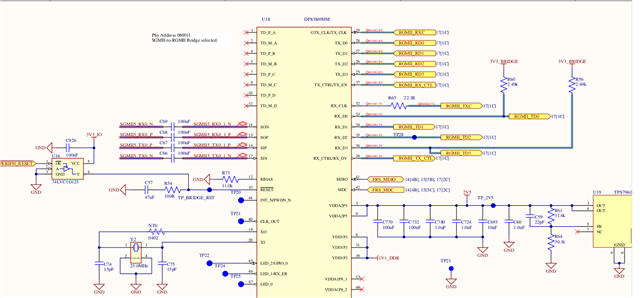
The ethernet topology is as follows:
cpsw9g (port5) <--> SGMII <--> DP83869 (addr 3) <--> RGMII <--> ADIN1100 (addr 0)
In our current DTS setup, we have defined the ADIN1100 as a child node under the DP83869 MDIO entry like this:
&main_cpsw0_mdio {
status = "okay";
main_phy3: ethernet-phy@3 {
reg = <3>; // DP83869
ti,op-mode = <DP83869_RGMII_SGMII_BRIDGE>;
adin1100: ethernet-phy@0 {
reg = <0>; // ADIN1100 behind DP83869
phy-mode = "rgmii";
};
};
};
Can you please confirm:
Is it valid to define ADIN1100 as a child node inside DP83869 like this?
Or should ADIN1100 be a separate sibling node under &main_cpsw0_mdio instead?
Appreciate your clarification on the correct binding for this bridging setup.
Thank you,
Dharanija.
