TDA4VM: Modify PCIE speed from GEN2 to GEN3 after TDA4 startup

Part Number: TDA4VM
Other Parts Discussed in Thread: AM69

Tool/software:

Hi,

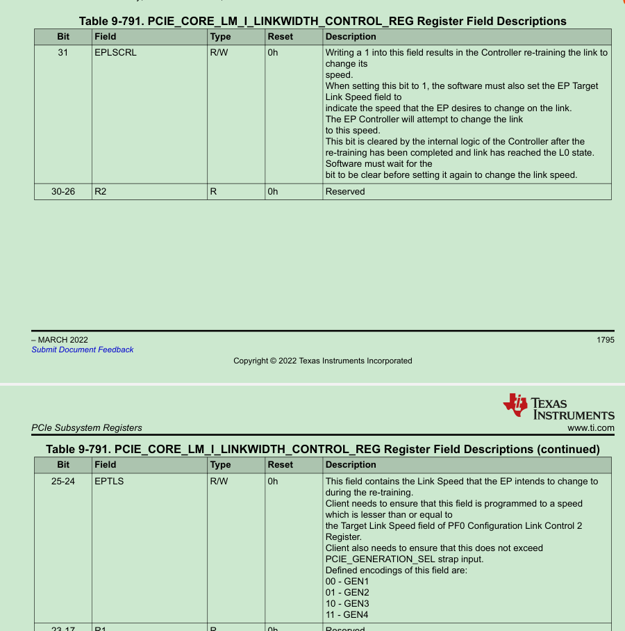
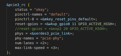
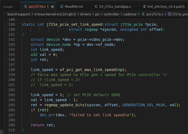
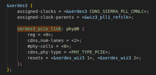
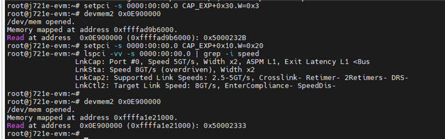
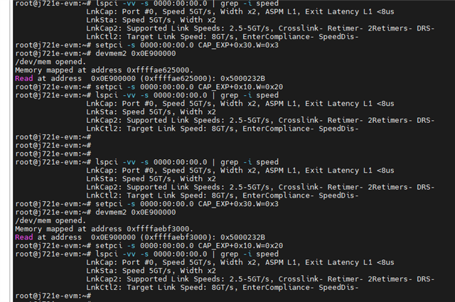
  Because if configured as GEN3 during startup, there is a probability that the external Switch chip cannot be recognized, resulting in driver loading failure. Therefore, GEN2 is defaulted during startup. Is there a way to modify the PCIE rate from GEN2 to GEN3 after TDA4 startup?

Regards,

Yang

  • Hi,

      May I ask if there is a corresponding solution to the above problem?

    Regards,

    Yang

  • Hi,

    Thank you for taking the time to post your question! I will look into this and get back to you within the next few days.

    Regards,

    Jeff

  • Hi,

    Thank you for your patience. The short answer is yes, the PCIe controller supports retraining the link to a different speed after startup. This can be done by writing to certain registers, such as PCIE_CORE_RP_I_LINKWIDTH_CONTROL_REG or PCIE_CORE_LM_I_LINKWIDTH_CONTROL_REG (depending on how you are accessing the PCIe controller and what role the controller is running in).

    Information about these registers can be found in part 4 of the register files for TDA4, DRA829TDA4VM_Registers_Part4.pdf (which can be downloaded here https://www.ti.com/product/TDA4VM#tech-docs , named "User Guide"). Information about those specific registers mentioned above can be found in that pdf on page 1725 for the LM register, and page 2254 for the RP register. 

    I hope this helps! Let us know if you have any other questions.

    Regards,

    Jeff

  • Hi,

      I have checked the register instructions and it seems to be set as an EP node. I am currently using the PCIE3 RP function. Which registers should I set?

    Regards,

    Yang

  • Hi,

    It also depends on the system you are operating in. For example, if you are using Linux, this following sequence should work:


    setpci -s 0000:00:00.0 CAP_EXP+0x30.W=0x3 - this changes target link speed to gen 3 speeds by setting link control 2 register
    setpci -s 0000:00:00.0 CAP_EXP+0x10.W=0x20 - this retrains the link by setting link control register's bit 5
    lspci -vv -s 0000:00:00.0 | grep -i speed - read the speed that is set as target speed and actual speed

    The bus number "0000:00:0.0" will be dependent on your hardware. You can use lspci command to check what is enumerated.

    Let us know if this helps or what system you are using to operate the controller. Thanks!

    Regards,

    Jeff

  • Hi,

      We are currently using Linux, and I have tried the command you sent. It can modify PCIE Speed to GEN3, but sometimes it takes multiple executions to

    succeed. Why is that?

    The following figure shows the default properties after power on:

    The following is the log that I have made multiple modifications to:

    Regards,
    Yang

  • Hi,

    LnkCap should be what the device is capable of operating at. In the first picture, the LnkCap of 5 GT/s for the TI device you are printing out might be a soft limit you set since hardware-wise, the J7 is capable of Gen3 speeds. Can you check your Linux devicetree and see what the max-link-speed is set to?

    max-link-speed = <3>;

    ^ This is what you want. <3> for Gen3.

    Regards,
    Jeff

  • Hi,

      Due to current functional limitations, I must keep PCIE at GEN2 during startup. Therefore, I manually set PCIE to GEN2 in the code, which results in Lnkcap

    being only 5GT/s during system startup. Is there any way to modify this property?

    Regards,

    Yang

  • Hi,

    I tried on AM69 just now as an experiment to see if I can retrain link to a speed greater than advertised in lnkcap register. Seems to link up to 8GT/s on first try. The issue might be somewhere else then.

    It may be an equalization phase issue during the retraining. Can you check the LnkSta2 register in PCIe config space that says whether certain equalization phases passed.

    Also, a lot of PCIe problems stem from clock issues, since both the root port and endpoint need to be properly synced to avoid issues.

    What is the clock configuration, refclk?

    What is the source for both J7 and the PCIe endpoint?

    Do they have a shared clock?

    Is it an external clock, or configured by J7 internally by its PLL?

    Regards,

    Jeff

  • Hi,

      The following is information about LnkSta2:

    What is the clock configuration, refclk?

      Yes, the current refclk is the default refclk inside the TDA4.

    What is the source for both J7 and the PCIe endpoint?

      EP is a MVL switch.

    Do they have a shared clock?

    Is it an external clock, or configured by J7 internally by its PLL?

      The clock configured by the PLL inside the J7.

    Regards,

    Yang

  • Hi,

    Hmmm, it appears that the link equalization failed or possibly never even started. The link must be in state L0 when equalization begins. Are you familiar with reading the TI registers of the PCIe controller? If so, there is a register that holds the value of the state the LTSSM is in. I am curious to know if the link is in the proper state of L0 when equalization begins. If you can find the controller base address, the LTSSM register offset is located in bits 29:24 of that register. That will tell you the state of the link. Can you read that register/memory after you set the new speed but before you set the retraining bit?

    Regards,

    Jeff

  • Hi,

      From the figure below, it can be seen that after setting the new speed, the register values did not change, but the register low bits changed after retraining.


      The following figure shows that the register value remains unchanged even when the speed modification fails.

    Regards,

    Yang

  • Hi,

    Thank you for the screenshots. I would like to go deeper into examining the state of the LTSSM. Could you poll the LTSSM field (bits 29:24 of PL_CONFIG_0) at a high enough frequency to catch all of the transient state changes of the LTSSM after retraining is initialized?

    Also, if you could mask those register bits (shift and zero out the unneeded bits), it would be easier to see the actual LTSSM state bitfield results. 

    So basically, once you initialize retraining to Gen3, start polling the LTSSM state register to see how it transitions from state to state.

    Regards,

    Jeff

  • Hi,

      I would like to know at what frequency do you expect to use to read this register value?

    Regards,

    Yang

  • Hi,

    If you could poll it every ~1ms, that would be a good place to start. a 5ms interval might be acceptable. You will enter different Recovery states as it progresses through link equalization. Also, continue to check LnkSta2 because it will show which stages of equalization were successfully completed (if any). 

    Below is a table from our TRM that shows the different states and the value that represents them in the register bitfield.

    Regards,

    Jeff

  • Hi,

      I will try the content later.

    Regards

    Yang

  • Hi,

    Here is a link to a thread that has more information about polling the LTSSM state. It also includes a bash script to do so.

     [FAQ] AM69: TDA4VH How to check current PCIe LTSSM state? 

    Regards,

    Jeff