SK-AM69: Help with enabling SERDES/ACSPCIe output on SK-AM69 (continued)

Part Number: SK-AM69
Other Parts Discussed in Thread: AM69

Tool/software:

This is a continuation of an older thread, which was locked due to inactivity:

SK-AM69: Help with enabling SERDES/ACSPCIe output on SK-AM69

Hi  , I'm sorry that I did not keep up with the older thread. In your last comment (here), you mentioned that you were in the process of trying to see if you could remove some circuitry from your SK-AM69 board to see if that is somehow having an effect. I'm guessing at this point that you either didn't have the time to try that yet, or it didn't make a difference for you -- but if you have any updates, please let me know.

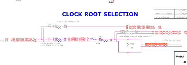
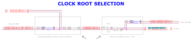
You recommended that we could copy what the SK-AM69 is doing with the external clock generation circuitry, but that is precisely what I am trying to avoid, due to the BOM cost that you mentioned, as well as the PCB space it would consume (every little bit counts). So I'm still looking for a way to give myself confidence that our AM69 PCB design will work without that additional circuitry.

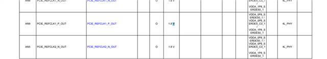
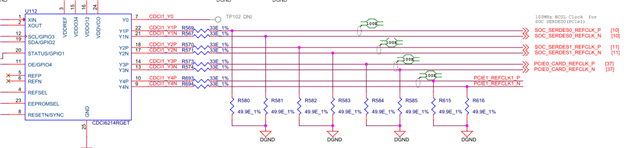
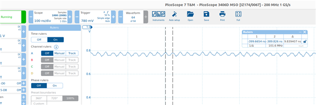
I was looking back over what we have done so far. Based on the oscilloscope screenshot that you posted in your last comment, it seems that you were able to add the 50Ω termination resistors to your board, because we are both seeing ~1.8V on TP106 after executing  devmem2 0x118090 w 0x01000002  in order to de-assert the power down bit for PCIe1.

I am thinking that perhaps this 1.8V could be a clue as to what is possibly being misconfigured inside the AM69. The SERDES REFCLK_OUT pins, such as AN9 which is connected to TP106, should be HCSL (High-Speed Current-Steering Logic), so that the output pin switches between driving 0mA (when "low") and ~14mA (when "high"). When that current is passed through the 50Ω resistor to ground, the resulting voltage at the test point should be either 0V (when "low") or ~0.7V (when "high"). At no point should an HCSL output pin exhibit a voltage of 1.8V, as far as I understand it. With TI's internal knowledge of the silicon, does it make any sense that 1.8V should be measured on these pins? Is there some misconfiguration of the SERDES that could make this happen?

Thanks for your continued help with this!

Best regards,
Dave

  • Sorry, I originally had the wrong title for this question -- I have corrected it to be, "Help with enabling SERDES/ACSPCIe output on SK-AM69 (continued)."

  • Hi Dave,

    I'm guessing at this point that you either didn't have the time to try that yet, or it didn't make a difference for you -- but if you have any updates, please let me know.

    Yes, you have guessed correctly. I was not able to make progress on this topic. But, I have it as one of my tasks in my todo list.

    I do have a J784S4 EVM board that I did some board mods to the connection of the PCIe reference clock which I can try out today/tomorrow. And in parallel, I can loop in some of the hardware folks to see if they have comments about the 1.8V.

    Regards,

    Takuma

  • Hi Takuma, I hope all is well. Just checking in to see if you have been able to make any progress, or if any of the hardware folks had thoughts about the 1.8V.

    If there is anything that I can do on my end to help you along, please let me know.

    Thanks and best regards,
    Dave

  • Hi Dave,

    Apologies for the delay.

    1.8V should be the logical high for that pin based on the datasheet:

    What I am seeing is the signal close to 1.8V, but slightly lower than 1.8V. I think this is due to the signal clocking at high frequency (1GHz) and not having enough time for the pin to go low.

    I did some board mods to remove the external clock input into the SerDes and tried some experiments, but still see clock at 1GHz. Suspecting that there is some divider within the SerDes module itself that is not being set up.

    Regards,

    Takuma

  • Hi Takuma, thanks for the reply. I have two thoughts/questions.

    1. I had also noticed that the "I/O Voltage" shown in that table is 1.8 V, but here is where my confusion lies from an electrical perspective. When that pin is functioning as a SerDes reference clock, to the best of my understanding, it should be operating in a HCSL (High-Speed Current-Steering Logic) mode. This means that when the pin is "high" it should be driving ~14mA of current through whatever load is connected. In our case, we have a 50Ω resistor to ground connected. Therefore, the voltage that we should be measuring at the pin when it is "high" is V = IR = ~0.014 * 50 = ~0.7 V. Then, even if there is not enough time for the pin to go low, it should be hovering around 0.7 V, not 1.8 V.
      1. I could be misunderstanding this, but if I am, can you please explain where my thinking is going wrong?
    2. Regarding the possibility that some divider within the SerDes might not be being set up, is there a SerDes expert that you could loop in on this to dig into the details and find out what needs to be done to correct the configuration? The problem I have is that I wouldn't know where to start to figure that out (and possibly the low-level information I would need isn't even available to me as an end user).

    Thanks for your continued support,
    Dave

  • Hi Dave,

    For SK-AM69, still having some issues getting 100MHz measured on the scope. I connected directly to the test point, and looking through schematics, the lack of termination resistors may be the reason why I am seeing voltage at near 1.8V.

    On the other hand, for J784S4 EVM, which is the automotive counterpart of AM69 and technically identical, I can measure a 100MHz reference clock for PCIe1 interface using the default SDK while probing C125. J784S4 TI EVM by default has J17 PCIe connector use internal reference clock, and SDK also reflects this hardware configuration.

    Regards,

    Takuma

  • If wanting the SK-AM69 to be configured for the processor to generate the REFCLK in place of the on-board clock generator (For SERDE0 / PCIe0)

    1. install 50-ohm termination resistors near source (R269, R275).  They are 'not installed' by default:

    2. Change REFCLK resistor mux so that REFCLK from processor connects to PCIe peripheral (and on-board clock generator is not connected) (Remove R405, R407, R403, R404), Install 0-ohm (R406, R408, C657, C658)

    Similar can be done for SERDES1 / PCIe0 (see schematic for specific reference designators)

  • Hi , are you sure that is the SK-AM69 schematic? I have the latest from https://www.ti.com/lit/zip/SPRR466 and it does not match what you have shown; for example, R269 is on the BOARD ID EEPROM sheet, and R405 is under LDOs.

  • Sorry for the confusion - I was looking at a different design.  The SK-AM69 supports only REFCLK from the CDCI device.  The clocks are connected to the SERDES_REFCLK pins, no the PCIe_REFCLK pins (ACSPCIe pins)

    The CDCI device is programmable - can support both HCSL and LVDS outputs.  I thought it default to HCSL, but would need to double check.  If Takuma is investigating the PCIe_REFCLK termination/configuration - that is not correct for this design.

    For the SK-AM69, the CDCI clock generator does have termination resistors near the source.

  •  , allow me to recap what I am trying to prove here. I am not actually trying to get the PCIe devices on the SK-AM69 to work with the PCIe_REFCLK pins (ACSPCIe pins).

    We are designing a custom PCB that is based on the SK-AM69. The custom PCB will not have the CDCI device on it. Instead, I need to use the PCIE_REFCLK0_P/N_OUT pins to generate the PCIe clock out to an endpoint on the custom PCB.

    We already have a custom build of the Processor SDK Linux for AM69 that we are able to load on the SK-AM69 today, and that we will eventually load on our custom PCB. Using our custom build of the Processor SDK Linux for AM69, I need to demonstrate that I can see the 100 MHz PCIe clock being generated on the PCIE_REFCLK0_P/N_OUT pins. On the SK-AM69, the PCIE_REFCLK0_P/N_OUT pins are connected to test points TP104 and TP105.

    Given that the PCIE_REFCLK0_P/N_OUT pins should be HCSL outputs, we have soldered a 50Ω termination resistor between TP104 and ground, and between TP105 and ground. With these termination resistors in place, I am expecting to see a 100 MHz clock being generated on TP104 and TP105, with an amplitude of approximately 0.7 V relative to ground.

    Using all available information from TI, including this E2E post and the previous one referenced above, we are confident that our custom build of the Processor SDK Linux for AM69 should be causing this 100 MHz clock to appear, but it is not.  then tried to reproduce my findings on his end with another SK-AM69, and he was seeing the same thing as me. We cannot get a 100 MHz clock to appear on TP104 and TP105. This is what I need to do in order to sign off on this aspect of the design of our custom PCB.

    I have been trying to solve this problem for about 4 months now. It was less urgent before, but our PCB design is nearing completion now, so I need to get to the bottom of it in short order. Thank you for the continued support.

    Best regards,
    Dave

  • Thanks for the clarification/status. I understand much better now.  I have Sk-AM69 board from Takuma and will add termination resistors.  We have this configuration working on another design, so it has been verified.  Just need to figure issue with Sk-AM69.

  •  , , thank you! I look forward to your findings. I doubt there is anything very helpful I can add on my end right now, but if you should need me to try anything here with my board, just let me know. -- Dave

  • Hi Dave,

    Looks like the termination resistors was the missing piece.

    In terms of raw register writes, below is what is needed:

    https://e2e.ti.com/cfs-file/__key/communityserver-discussions-components-files/791/3113.enable_5F00_internal_5F00_ref_5F00_clock_5F00_out_5F00_pcie1_5F00_j784s4.patch

    But the driver should handle these writes through dts.

    Regards,

    Takuma

  •  and , at long last I can confirm that I am seeing the reference clock being generated on my SK-AM69 board! And yes, the driver was handling the configuration through dts; with the dts changes, I did not need to do manual register accesses.

    And what was the problem, you might ask? When we went to add the 50 Ω termination resistors to our board a few months back, the resistors that we used were accidentally 50 kΩ. man facepalming

    When we changed them to 50 Ω today, the reference clocks appear on the oscilloscope as expected.

    Thanks very much for your help throughout this case and for confirming the correct behavior on your end, because that's what spurred me on to find the problem with my board. Again, it's very appreciated.

    Best regards,
    Dave

  • Hi Dave,

    Glad we could sort this out! Thank you   and  !

    Regards,

    Takuma