This thread has been locked.

If you have a related question, please click the "Ask a related question" button in the top right corner. The newly created question will be automatically linked to this question.

AM625: Serial resistor on MMC_CLK

Part Number: AM625


Tool/software:

There is confliction on either schematic design guidelines and checklist: 

https://www.ti.com/lit/pdf/sprad21

https://www.ti.com/lit/pdf/sprado3

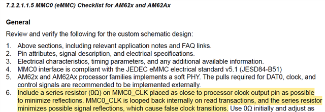
#1. In Section 5.2.1.5, it highlighted MMCx and OSPI interface doesn't need series resistor on clock. But in later 7.2.2.1.1.5, it is highlighted to include one. 

#2. Customer's question:

How the AM62x internally samples eMMC_CLK during eMMC read operations, and what state does eMMC_CLK need to reach for accurate sampling by the AM62x? This concern arises because the eMMC_CLK signal is sent from the source. When sampled at the source, the physical characteristics of the PCB dictate that the signal will inevitably have middle level steps, and the slew rate does not meet the AM62x's requirements.

  • Hello Tony, 

    Thank you for the query.

    Please read the full para. See highlighted below.

    5.2.1.6 Peripheral Clock Output Series Resistors

    Series resistor on the clock output near to the processor clock output pin is required to resolve issues with signal distortion at the source of the clock since the clock output is also used for retiming. For MMCx and OSPI interface an unbonded pad is used (internal),so series resistor is not a requirement. In some cases, a low value series resistor is added for signal integrity purpose. The recommendation is to have the series resistor as a place holder just in case the resistor is needed for improving signal integrity

    A series resistor is recommended for SPI and McASP clock output since the clock output is looped back from the PAD for retiming during data received.

    The above para says the series resistor is not a requirement for MMCx and OSPI/GMPC.for retiming. The clock is internally buffered and used for data receive,

    We are still recommending customer to provision a 0R for control of reflection. The same is reflected in the checklist.

    Regards,

  • We read the full para. we are asking the 7.2.2.1.1.5 is conflicted with 5.2.1.5. 

    Paul,

    How do you think?

  • Hello Tony, 

    Thank you.

    The below para is the guidelines 

    5.2.1.6 Peripheral Clock Output Series Resistors

    Series resistor on the clock output near to the processor clock output pin is required to resolve issues with signal distortion at the source of the clock since the clock output is also used for retiming. For MMCx and OSPI interface an unbonded pad is used (internal),so series resistor is not a requirement. In some cases, a low value series resistor is added for signal integrity purpose. The recommendation is to have the series resistor as a place holder just in case the resistor is needed for improving signal integrity.

    The below is the checklist.

    Include a series resistor (0Ω) on MMC0_CLK placed as close to processor clock output pin as possible to dampen reflections. MMC0_CLK is looped back internally on read transactions, and the resistor eliminates possible signal reflections, which cause false clock transitions. Use 0Ω initially and adjust as required to match the PCB trace impedance

    Please refer to the sentences in bold.

    I am not sure where you are seeing conflict?

    Regards,

    Sreenivasa

  • Hello Tony, 

    We are in the process of updating the checklist.

    Below will be the new guidelines

    Series resistor on the clock output near to the processor clock output (MCSPI, MCASP) pin are recommended for probable reflection control (signal distortion) at the source of the clock output since the clock is also being used for retiming.

    For MMC0, MMC1, MMC2, OSPI0, GPMC0 interfaces, an unbonded pad is used (internal). A low value series resistor (0Ω to start)  is recommended (provisioned) to control possible signal reflections (signal integrity purpose).

    Regards,

    Sreenivasa

  • Okay, that will look better.

    How about the second question. That is what customer really concerned. 

  • Hello Tony,

    Thank you.

    How the AM62x internally samples eMMC_CLK during eMMC read operations, and what state does eMMC_CLK need to reach for accurate sampling by the AM62x? This concern arises because the eMMC_CLK signal is sent from the source. When sampled at the source, the physical characteristics of the PCB dictate that the signal will inevitably have middle level steps, and the slew rate does not meet the AM62x's requirements.

    There is a MMC0_CLKLB signal is not pinned out on the device which is a buffered version of MMC0_CLK that is used during read.

    I will request Paul to add his thoughts.

    Regards,

    Sreenivasa

  • Update from offline:

    #1. "The clock is looped back, so the first part of the comment is true.  However, the loopback is done via an unbounded IO.  So, the second half of the comment is not true."

    #2. We do not use the same clock that is sent across the PCB to the attached device for our capture clock.  We branch the output clock into two paths inside the device, where the clock is sent to two separate IO cells.  One IO cell is connected to a package ball, which is used to source a clock to the attached device.  The other IO cell is unbounded (not connected to any package ball).  The clock we use as the receive capture clock is sent out through the unbounded IO cell and looped back into the device before being used as the capture clock.  We do this so the clock has the same delay that is inserted on the clock going out to the attached device and the same delay that is inserted on the data coming back in from the attached device.  The unbonded IO cell pad never experiences the voltage step that is produced on the source end of a PCB signal trace.

  • hello Tony,

    Thank you for adding the comments.

    Regards,

    Sreenivasa