J721S2XSOMXEVM: GPIO: Unable to see the GPIO toggle on the Logic Analyzer / Scope

Part Number: J721S2XSOMXEVM
Other Parts Discussed in Thread: TCA6424

Tool/software:

Hi,

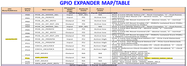
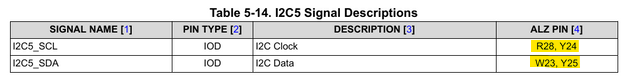
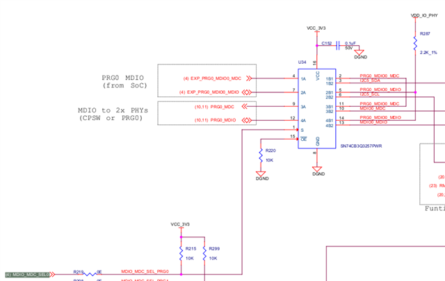
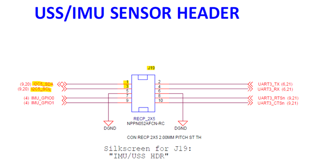
I have set the Pinmux Config to GPIO for Pins(Y25, R28, W23, Y24), as I am not really sure which two out of those four are actually mapped to the J19 connector on GESI Board

I could see that the registers are configured as expected, and the GPIO output is also updated on the GPIO0_MEM_OUT_DATA01, as well as GPIO0_SET_* and GPIO0_CLR_* registers.

So, my expectation is I should be able to see the I2C5_SCL(R28 or Y24) and I2C_SDA(Y25 or W23) toggle from high to low and low to high, but I don't see any change on the Scope.

I suppose only the *SET* and *OUT* should show the expected output and *CLR* should be opposite to *SET*. If that is how it is supposed to be, then it looks like for some reason SET and CLR instructions are happening at almost next to each other, which makes the pin always stay low.

Could you kindly let me know, if I miss something or how could I get it to work?

I am using,

  • J721S2 SOM (PROC118E3)
  • GESI Card (PROC084A)
  • Jacinto 7 CPB (PROC079A)
  • PDK 11.0.0.21
  • Baremetal GPIO Blink code is modified accordingly.

Thanks.

Best,
Moses

  • Hi Moses,

    Could you please provide a dump of the GPIO registers? Additionally, could you also provide the padconfig register?

    I suppose only the *SET* and *OUT* should show the expected output and *CLR* should be opposite to *SET*. If that is how it is supposed to be, then it looks like for some reason SET and CLR instructions are happening at almost next to each other, which makes the pin always stay low.

    Take a look at the following snippet from the TRM for more information on the SET and CLR registers:

    Thanks,

    Neehar

  • Hi Neehar,

    For GPIO0_6 and GPIO0_7 from MAIN domain; both of those GPIOs are configured as Outputs

    Here is the Pinmux config, 

    0x0011C018 CTRL_MMR0_CFG0_CFG0_PADCONFIG6
    0x0011C018 0x07 0x00 0x05 0x00
    0x0011C01C CTRL_MMR0_CFG0_CFG0_PADCONFIG7
    0x0011C01C 0x07 0x00 0x05 0x00

    Here are the GPIO Regs when both of those GPIOs are set(high),
    0x00600000 GPIO0_MEM_pid
    0x00600000 0x05 0x29 0x83 0x44
    0x00600004 GPIO0_MEM_PCR
    0x00600004 0x01 0x00 0x00 0x00
    0x00600008 GPIO0_MEM_BINTEN
    0x00600008 0x01 0x00 0x00 0x00 0x00 0x00 0x00 0x00
    0x00600010 GPIO0_MEM_DIR01
    0x00600010 0x3F 0xF7 0xFF 0xFF
    0x00600014 GPIO0_MEM_OUT_DATA01
    0x00600014 0xC0 0x08 0x00 0x00
    0x00600018 GPIO0_MEM_SET_DATA01
    0x00600018 0xC0 0x08 0x00 0x00
    0x0060001C GPIO0_MEM_CLR_DATA01
    0x0060001C 0xC0 0x08 0x00 0x00
    0x00600020 GPIO0_MEM_IN_DATA01
    0x00600020 0xFF 0xFF 0x9F 0xFF
    0x00600024 GPIO0_MEM_SET_RIS_TRIG01
    0x00600024 0x00 0x08 0x00 0x00
    0x00600028 GPIO0_MEM_CLR_RIS_TRIG01
    0x00600028 0x00 0x08 0x00 0x00
    0x0060002C GPIO0_MEM_SET_FAL_TRIG01
    0x0060002C 0x40 0x00 0x00 0x00
    0x00600030 GPIO0_MEM_CLR_FAL_TRIG01
    0x00600030 0x40 0x00 0x00 0x00
    0x00600034 GPIO0_MEM_INTSTAT01
    0x00600034 0x00 0x00 0x00 0x00

    Here are the GPIO Regs when both of those GPIOs are cleared(low),
    0x00600000 GPIO0_MEM_pid
    0x00600000 0x05 0x29 0x83 0x44
    0x00600004 GPIO0_MEM_PCR
    0x00600004 0x01 0x00 0x00 0x00
    0x00600008 GPIO0_MEM_BINTEN
    0x00600008 0x01 0x00 0x00 0x00 0x00 0x00 0x00 0x00
    0x00600010 GPIO0_MEM_DIR01
    0x00600010 0x3F 0xF7 0xFF 0xFF
    0x00600014 GPIO0_MEM_OUT_DATA01
    0x00600014 0x00 0x00 0x00 0x00
    0x00600018 GPIO0_MEM_SET_DATA01
    0x00600018 0x00 0x00 0x00 0x00
    0x0060001C GPIO0_MEM_CLR_DATA01
    0x0060001C 0x00 0x00 0x00 0x00
    0x00600020 GPIO0_MEM_IN_DATA01
    0x00600020 0x3F 0xF7 0x9F 0xFF
    0x00600024 GPIO0_MEM_SET_RIS_TRIG01
    0x00600024 0x00 0x08 0x00 0x00
    0x00600028 GPIO0_MEM_CLR_RIS_TRIG01
    0x00600028 0x00 0x08 0x00 0x00
    0x0060002C GPIO0_MEM_SET_FAL_TRIG01
    0x0060002C 0x40 0x00 0x00 0x00
    0x00600030 GPIO0_MEM_CLR_FAL_TRIG01
    0x00600030 0x40 0x00 0x00 0x00
    0x00600034 GPIO0_MEM_INTSTAT01
    0x00600034 0x00 0x00 0x00 0x00

    Best,
    Moses

  • Hi Moses,

    Thanks for the dump of the GPIO registers.

    So, my expectation is I should be able to see the I2C5_SCL(R28 or Y24) and I2C_SDA(Y25 or W23) toggle from high to low and low to high, but I don't see any change on the Scope.

    Before this, can you confirm if you are setting the MDIO_MDC_SEL0?

    Based on the GESI board schematic, this select bit is used to mux I2C5, using chip U34, out to the headers. The MDIO_MDC_SEL0 is set by controlling the GPIO Expander via the I2C0 bus. This may be why you are unable to see any output on the I2C5 bus.

    Thanks,

    Neehar

  • Hi Neehar,

    Unfortunately that didn't seem to work. I have configured the MUX2_EXP pin (P15) as exepected,

    Wrote 0xDF to 0x07

    and 0xDF to 0x03 (Low) or 0xFF  to 0x03 (High)

    I have tried setting the output pin (MUX2_EXP or MDIO_MDC_SEL0) to both High and Low, and in both cases I see no change on the I2C5 lines.

    Best,
    Moses

  • Hi Moses,

    Can you confirm if the MDIO_MDC_SEL0 is set to high with a scope?

    Additionally, can test if you can control the TCA6424 GPIO expander using the I2C0 bus as well as it is address 0x22 on the bus?

    Thanks,

    Neehar

  • Hi Neehar,

    Can you confirm if the MDIO_MDC_SEL0 is set to high with a scope?

    I'd have to check that. I have only verified that this Pin is set as Output and High, by reading the 16pin GPIO Expander's registers.

    Additionally, can test if you can control the TCA6424 GPIO expander using the I2C0 bus as well as it is address 0x22 on the bus?

    The MDIO_MDC_SEL0 is on I2C0 0x20, right?
    But to answer your question, Yes, I can control the 24pin GPIO Expander. I am able to toggle the USER_LEDs on I2C0 0x22.

    Thanks.

    Best,
    Moses

  • Can you confirm if the MDIO_MDC_SEL0 is set to high with a scope?

    Yes, I confirm that this pin is set to High using a Scope.

  • Also, as I dont have the complete PCB Layout / Design files, how do I know the respective i2c pins are connected to which balls?

  • Hi Moses,

    Thanks for your responses and details.

    You can refer to the datasheet for information on what signals are connected to which balls.

    Can you also provide a dump of the pinmux registers for the pads that you use?

    Thanks,

    Neehar

  • Hi Neehar,

    Yes the above picture with Ball info is from the same datasheet.I have tried with both of the ALZ pins on two trials.
    For GPIO I have used the mode 7 on all of them, and for I2C it is 8(W23,Y24) and 13(Y25, R28)
    I am initially trying to check if GPIO works, which didn't seem to be the case, then I have used the example GPIO Led Blink almost as is, except, now I have GPIO toggle in a while loop to debug; and checked the TP45 on CPB, which is supposed to be WKUP_GPIO0_6, even that doesn't seem to toggle. There seems to be some general issue with GPIO then?

    Thanks.

    Best,
    Moses

  • Hi Moses,

    Could you provide the dump of the pinmux registers? There are some bits other than the muxmode that are important as well that could be causing issues.

    Thanks,

    Neehar

  • Hi Neehar,

    Sure as posted earlier w/ the GPIO regs, the padconfig is set as following for the GPIO mode,
    0x0011C018 CTRL_MMR0_CFG0_CFG0_PADCONFIG6
    0x0011C018 0x07 0x00 0x05 0x00
    0x0011C01C CTRL_MMR0_CFG0_CFG0_PADCONFIG7
    0x0011C01C 0x07 0x00 0x05 0x00

    Thanks,
    Moses

  • Hi Moses,

    Sorry I did not realize you had provided it earlier. Let me look into this further and get back to you.

    Thanks,

    Neehar

  • Hi Neehar,

    I have checked with two J721S2 SOMs and in both cases it didn't work.
    I happen to have a J721ESOM as well with me and I tried to check the gpios &/ i2c5, spi3 pins, they all responded as expected.
    Same GESI board, same CPB, just a different SoM. 

    Could it be that there is some bug in the preprocessor statements for the J721S2?

    Thanks.

    Best,
    Moses

  • Hi Moses,

    Thanks for the details and further information from your tests. I will look into this deeper and get back to you tomorrow.

    Thanks, 

    Neehar

  • Hi Neehar,

    Any updates on this issue?

    Thanks,
    Moses

  • Hi Moses,

    Our expert is OoO and he will support you next week.

    Regards,

    Karthik

  • Hi Moses,

    Sorry for the delays as I was out of office and catching up.

    I have looked deeper into the schematics for the SOM, CPB, and GESI board and it seems the source signals for I2C5_SCL and I2C5_SDA are not outputted from the J721S2 SOM. The signal is outputted from the GESI board using the Mux I have shown below with the select bit MDIO_MDC_SEL0 as we discussed before.

    However, PRG0_MDIO0_MDIO and PRG0_MDIO0_MDC are the sources for I2C5_SCL and I2C5_SDA respectively from the SOM, through the Common Processor Board (CPB), and to the GESI board. The SOM to CPB connector for J721S2 does not output the source signals for PRG0_MDIO0_MDIO and PRG0_MDIO0_MDC as shown in the image below. It is expected on pins F19 and G22.

    I also compared this to the J721E SOM and you can see the signal is connected through the SOM, to the CPB, and all the way to the GESI board as shown in the images below on pins F19 and G22.

    SOM to CPB connection:

    CPB to GESI connection:

    Since it is not connected, you will not be able to use I2C5_SCL or I2C5_SDA on the GESI board with the J721S2 SOM. Feel free to reach out if you have any further questions.

    Thanks,

    Neehar