This thread has been locked.

If you have a related question, please click the "Ask a related question" button in the top right corner. The newly created question will be automatically linked to this question.

AM620-Q1: Input Slew Rate

Part Number: AM620-Q1
Other Parts Discussed in Thread: PCA9306, AM6442

Tool/software:

Hi,

I am using AM6204 and would like to clarify on some peripheral input slew rate specification.

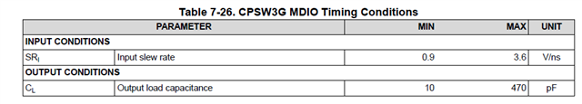
  1. In my device, the actual measured input slew rate for MDIO is 0.14V/ns, which is not within range of 0.9V/ns ~ 3.6V/ns as specified in Table 7-26. CPSW3G MDIO Timing Conditions. The maximum data rate of MDIO for my application is only 625kHz.
  • Is the Input slew rate specification in Table 7-26 applicable to higher data rate e.g. 5MHz only?

  • Can i refer to input slew rate in 7.8.6 LVCMOS Electrical Characteristics for my application? E.g. input slew rate specification = 33fV/ns = 0.0206V/ns?

2. For SPI data input, the actual measured input slew rate is 1.45V/ns, which is not within range of 2V/ns ~ 8.5V/ns as specified in Table 7-74. MCSPI Timing Conditions.The maximum data rate of SPI for my application is only 10MHz. Similarly, can i refer to input slew rate in 7.8.6 LVCMOS Electrical Characteristics for my application? E.g. input slew rate specification= 33fV/ns = 0.33V/ns?

3. For Enhanced Capture (ECAP) Input, the actual measured input slew rate is 0.04V/ns, which is not within range of 1V/ns ~ 4V/ns as specified in Table 7-45. ECAP Timing Conditions. The maximum data rate of ECAP for my application is only 1Hz. Similarly, can i refer to input slew rate in 7.8.6 LVCMOS Electrical Characteristics for my application? E.g. input slew rate specification = 3.3MV/s?

4. For GPIOx, in my application the toggling frequency is below 10kHz. shall i refer to the input slew rate in 7.8.6 LVCMOS Electrical Characteristics for my application? E.g. input slew rate = 3.3MV/s?

There is another GPIO timing specification in Table 7-59. GPIO Timing Conditions, is this for high toggling frequency application only? What is value for functional clock period?


5. What are the impacts if the input slew rate specification is not satisfied? 

  • Hello Khor Boon Tiang,

    Thank you for the query.

    The minimum Input Slew Rate parameter defined in each Electrical Characteristics table is associated with long-term reliability. 

    The minimum Input Slew Rate parameter defined in each peripheral timing section is a requirement to meet the respective peripheral timing parameters.

    The device may not work as expected if you violate the minimum input slew rate limit defined in the respective peripheral timing section, but the device could be permanently damaged if you violate the minimum input slew rate limit defined in the respective Electrical Characteristics table. It is very important that you minimize the time a signal connected to one of our input buffers spends in the mid-supply region as it transitions from low to high or high to low.

    I assume this is a custom board.

    Can you please share the waveforms.

    Do you have series resistors of filters on the signals. Are you able to share the schematics for a quick check.

    Kind Regards,

    Anastas Yordanov

  • Hello Khor Boon Tiang,

    Please note the updates to the previous message.

    Regards,

    Sreenivasa

  • Yes, this is custom board.

    Below is the MDIO and MDC waveform.

    sorry not able to share schematic due to confidential. there is no series resistor but MDIO is connected to Voltage translator PCA9306 with external pull up 1K ohm.

    From this FAQ --> [FAQ] AM6442: Minimum value of UART Input Slew Rate - Processors forum - Processors - TI E2E support forums. It gave hint that minimum input slew rate defined in the Chapter 7.11.5 Peripheral is required to achieve the maximum data rate.

    Can i refer to input slew rate specification in chapter 7.7.6 LVCMOS electrical characteristics? It has toggling frequency which is closest to my actual application.

    Regards,

    Khor

  • Hello Khor, 

    Are you seeing any functional issue,

    Help me understand the trace length of the MDIO that is causing the loading.

    The peripheral slew rate is for performance and the LVCMOS IO slew rate is for IO reliability.

    Regards,

    Sreenivasa

  • Hi Sreenivasa, 

    No issue seen so far as still in early development phase.

    The trace length of MDIO is about 45mm and it is 50-ohm impedance-controlled. 

    I tried to understand the relationship between the slew rate limit with data rate.

    Signal Maximum data rate [bps] 7.8.6 LVCMOS Slew Rate
    = 33*f [V/ns]
    Respective peripheral specification in Chapter 7.11 [V/ns]
    UART 12,000,000 0.396 0.5 ~ 5
    MDIO 2,500,000 0.0825 0.9 ~ 3.6
    MSPI 50000000 1.65 2 ~ 8.5

    For UART and MSPI, the peripheral slew rate is close with the LVCMOS slew rate if using the formula 33*toggle frequency.  

    Could you please help to confirm the maximum data rate on MDIO that used for peripheral slew rate limit?

    Since my application do not use maximum data rate, is it make sense to re-consider the peripheral slew rate limit based on actual input toggle frequency instead of maximum data rate?

    Regards,

    Khor

  • Hello Khor, 

    Thank you.

    I checked with the expert.

    The recommendation is to follow the slew rate requirements mentioned for each of the peripherals when the LVCMOS IOs are configured for specific functionality.

    Regards,

    Sreenivasa

  • Hi Sreenivas, 

    Noted with thanks.

    May i know what is the period for functional clock as specified in GPIO timing requirement?

  • Hello Khor, 

    Thank you.

    MAIN_SYSCLK0 (SYSCLK0) -- 500 MHz (Derived from MAIN PLL 0)
    MCU_SYCLK0 -- 400 MHz (Derived from MCU PLL 0)

    Note: You need to use the Clock tree tool to get the clock period for each peripheral where the functional clock period is reference.

    Regards,

    Sreenivasa