This thread has been locked.

If you have a related question, please click the "Ask a related question" button in the top right corner. The newly created question will be automatically linked to this question.

OMAP-L138: VDD capacitor placement in relation to the ferrite beads for OMAP's clock source

Part Number: OMAP-L138

Tool/software:

Hi team,

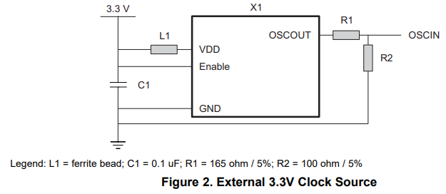
In the Errata Section 2.1.4, it is mentioned that the VDD filter ferrite beads and capacitor should be placed as the figure below into the clock source. 

Question 1: Should C1 be placed before the beads as shown in the diagram, or should it be placed after the beads as close to the VDD pin as possible?

Question 2: Where is the ESD source assumed to be in the diagram below? (I assume the 3.3V line)

Best Regards,

Yu

  • You are correct. Connecting the device as shown would not be a good design practice. This connection topology is likely to cause the clock source power supply to be very noisy and potentially compromise the performance of the clock source. The filter should be implemented as a pi-type low pass filter, where there is a bulk capacitor on both sides of the ferrite bead as well as a high frequency capacitor placed on the clock source side of the ferrite bead.

    I will request an update to the diagram.

    Regards,
    Paul