Hi,
I would like to ask some questions with OMAP L138 DDR2 controller DQGATE routing.
Length

I found that there is some ambiguity in the expression for CKB0B1. Does “CK net” refer to a net class or nets?
- To interpret it as CK net class, we have support in Table 5-33;
- To interpret it as a net, we note that
(1) “CK” net class comprises unidirectional {DDR_CLKP, DDR_CLKN} differential pair which runs in close parallel from L138 DDR2 controller to DRAM, and is not a loopback signal, so there is no physical/electrical motivation in adding their lengths without an averaging division by 2.
(2) The expression uses singular form “net” in “CK net”, but plural form “nets” in “DQS0 and DQS1 nets”, so I guess the author was probably suggesting using either DDR_CLKP or DDR_CLKN since both ∊ {CK net class} and length(DDR_CLKP) ≈ length(DDR_CLKN), therefore picking either is fine.
To ascertain the correct interpretation, I measured net lengths related to CKB0B and DQGATEF in L138 datasheet Fig. 2-25.

I found that the approximate equality holds (within 100mil DQGATE skew) only when we interpret CK net length as
✓ CKnet length ≡ ∑(DDR_CLKP, DDR_CLKN)/2
However, if we interpret CK net length as
✕ CKnet length ≡ ∑(DDR_CLKP, DDR_CLKN)
The skew would be over 1900mil.
Therefore I think “CK net length” should not be interpreted as the sum of DDR_CLKP & DDR_CLKN, which are members of “CK net class”, but should be either of them, or the average of them.
Could anyone confirm this?
Resistor

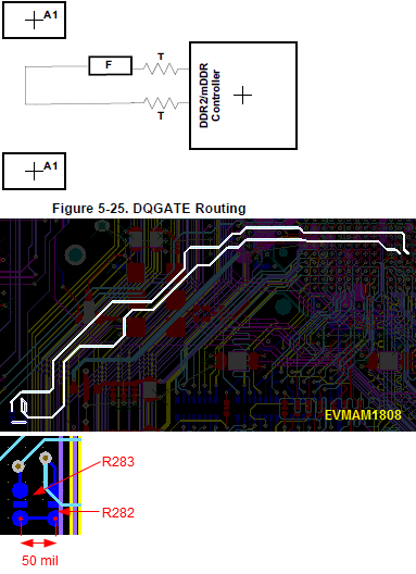
In L138 datasheet Fig. 5-25:
Does T refer to termination resistors?
- The drawing show two T’s as being physically close to memory controller, whereas on EVMAM1808 the two resistors R282 and R283 situated very far from the memory controller (part of AM1808). Which one is correct?
- If the placement of EVMAM1808 is correct (being the only correct and Fig. 5-25 wrong, or both correct and EVAMA1808 R282 & R283 placement are valid implementation of Fig. 5-25), then since they are very close (measured distance between centerof connecting pads being 50mil), can they be combined into one?
- Since the allowed DQGATE skew, per Table 5-38, is only 100mil, the 50mil pad-to-pad center distance becomes significant here and cannot be ignored. Should I count DQGATE length F including this pad-to-pad distance? If yes, should I count from the center of two pads, or the edge of two pads which would be significantly smaller?
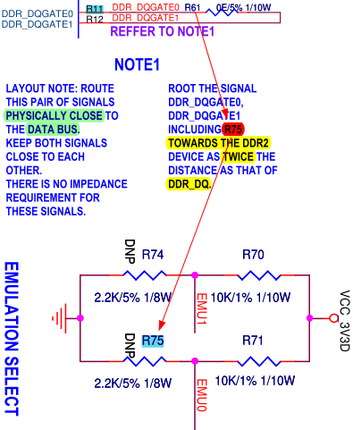
In Hawkboard_schematics_v1, there are expressions like
(1) Toward DDR2
(2) Twice the distance as that of DDR_DQ
(3) Physically close to data bus

I don’t understand this, especially (2). Could anyone explain this?
In addition, the resistor in Hawkboard v1 between DDR_DQGATE0 and DDR_DQGATE1 is R61, whereas Note 1 refers to R75 which actually belongs to the emulation part. I think it is erroneous. Could someone confirm this?
Shape

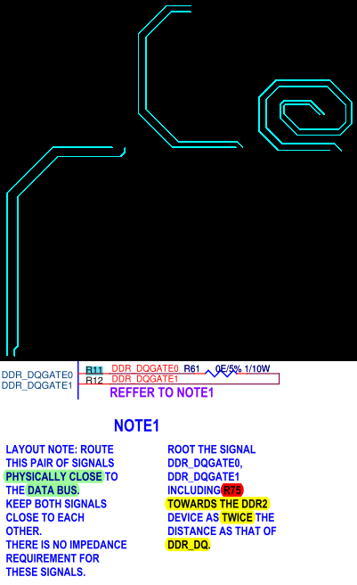
To meet the length requirement (depending on the answer of “Length” above), CAD tools offer different ways for tuning the length when straight or normally bended traces cannot have enough length within a particular region. There are different ways of length tuning: rounded, Mitered with Lines, Mitered with Arcs, etc.
In addition, although {DDR_DQGATE0, DDR_DQGATE1} are not differential pairs, tools/techniques for tuning differential pairs can also be used for tuning their length, resulting in approximately equal lengths for the two nets while also satisfying their ∑(length) requirement.
However, in either EVMAM1808 or Hawkboard, I didn’t see {rounded, Lines/Arcs-Mitered} traces for {DDR_DQGATE0, DDR_DQGATE1}. For example, EVAMA1808 uses weakly bended traces for them. But on a board where the space is rather limited, may I choose to use these mitering techniques? Are these shapes valid for {DDR_DQGATE0, DDR_DQGATE1}?
Orientation
I am also confused on why Hawkboard_schematics_v1 suggested routing “toward” the DDR2, in addition to other questions asked under Q.Resistors above. If {DDR_DQGATE0, DDR_DQGATE1} is just a loopback signal for external DQS gating as defined in Table 2-10, p.37, why restrict its orientation?
For example, within limited space the traces might opt to wind in any of the orientations below. Is there any reason why one is allowed and others are not? Why it has to go toward DDR2?

A1

In various figures I see “A1”being used, however a search in datasheet finds no definition prior to usage. Does “A” stand for “area”? However, what does “1” mean? In these figures it seems that there are two memories, but why the second is not called “A2”?
Zheng

