


Other Parts Discussed in Thread: TDA4VH
Tool/software:
What is the recommended placement for the 50ohm termination resistors on PCIe REFCLK_P/REFCLK_N when REFCLK is used as output from TDA4VH SoC to the peripheral?
We are simulating PCIe REFCLK with Hyperlynx and using standard SERDES models to generate 100MHz differential clock.
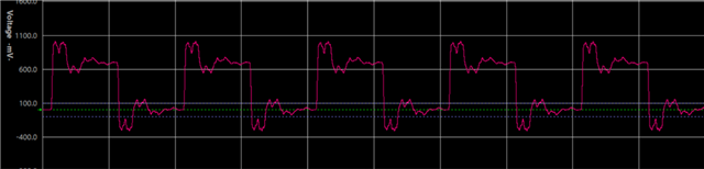
When placing the 50ohm termination resistors close to the SoC as suggested by Jacinto7 AM6x, TDA4x, and DRA8x High-Speed Interface (spracp4a) and TDA4VH EVM design we get the following signal waveform:
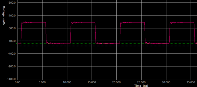
But when removing the termination resistors from close to the SoC and placing them next to the peripheral (receiver) we get the following signal waveform, which looks more like what would be expected.
Is TDA4VH PCIE_REFCLK output different in this case that the termination resistors should still be close to SoC (transmitter) and not close to peripheral (receiver)?
If so, would you have simulation model PCIE_REFCLK?
