AM5716: security boot key burning issue, how to implement VPP power supply

Part Number: AM5716
Other Parts Discussed in Thread: DRA716

Tool/software:

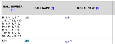
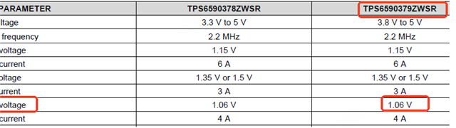
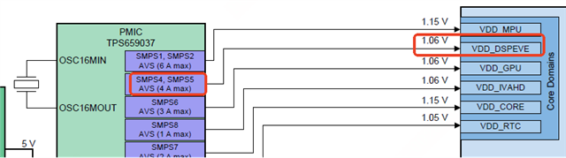
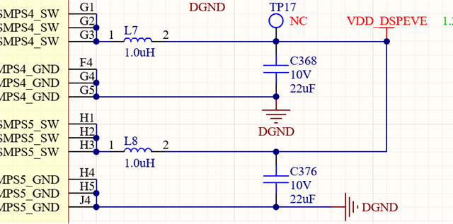
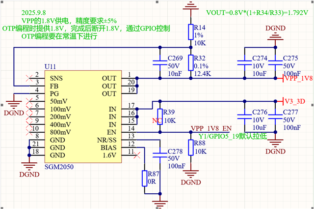
使用TLV70718还需要新增一个器件,我们想使用已有的TPS6590379ZWSR来给VPP供电,该怎样实现?

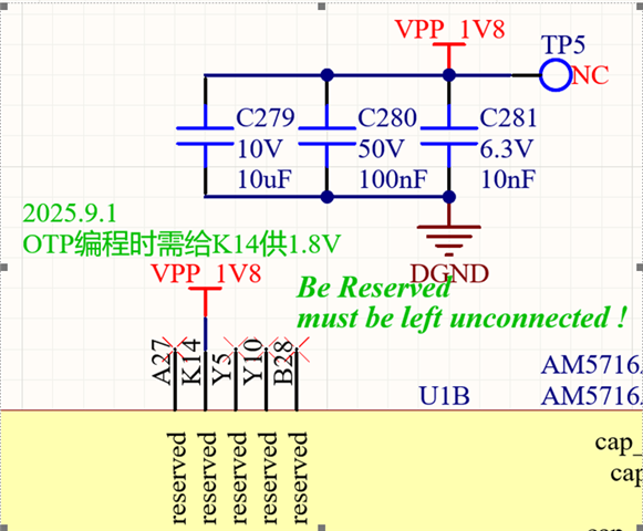
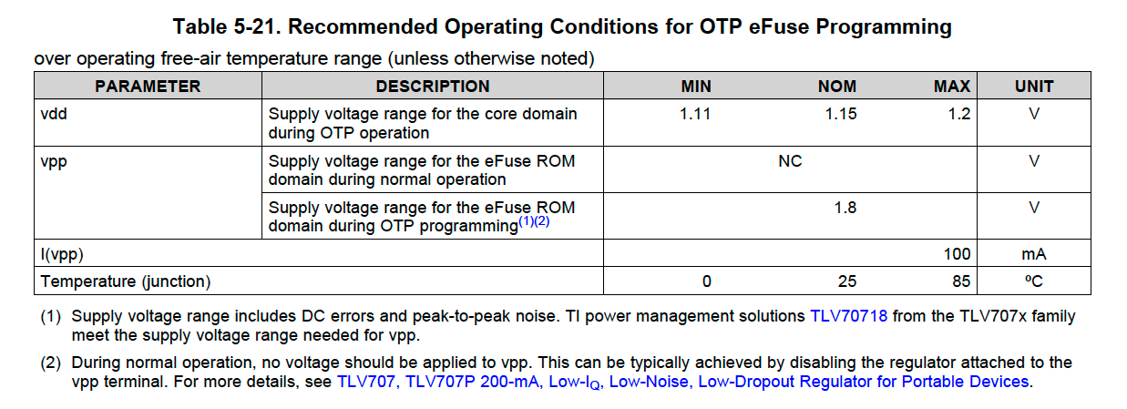
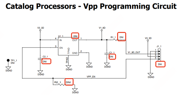
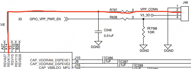
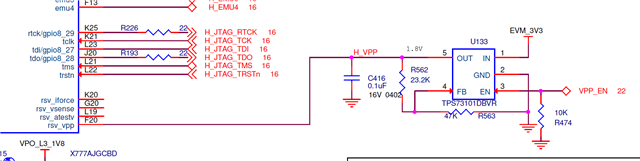
in the security boot document, it recommends customer to use TLV70718 to provide VPP power, but in customer design of AM5716 HW board,

there is no such device, if add a new TLV70718 device, it needs customer to re-design the HW, this is a big change, 

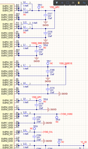
in customer AM5716 GP board, it use TPS6590379ZWSR as power supply solution,

is it possible customer to use TPS6590379ZWSR to provide power to VPP?

    please help check it.

Thanks

   Semon

  • Hi Semon,

    Do they have any unused/spare rails/LDOs on their TPS6590379 PMIC?

    Another approach would be to use a test point and provide power from an external supply (from their ICT?) during efuse programming.

    REgards,

    Kyle

  • Hi Chen 

         please refer to this AM574x security boot design, it includes VPP supply design.

         3487.AM574X_INDUSTRIAL_EVM_SCH_1_0A.pdf

    Regards

       Semon

  • Hi Kyle

    in the AM574X diagram, 1.8V circuit is DNI, so where does VPP come from, where is J46 connected to?  

    could you help give some explanation about this solution?

    Thanks

       Semon

  • Hi Semon,

    The DRA716 EVM provides a more straightforward implementation:

    https://www.ti.com/tool/DRA71XEVM#design-files

     \

    As an alternative, does the customer PCB have an available test point on F20 (vpp)?  They may be able to use an external power supply to source VPP.  They should validate that any solution is able to keep the supply level within the datasheet spec range (1.8V+/-5%) during efuse programming.

    Regards,

    Kyle

  • As an alternative, does the customer PCB have an available test point on F20 (vpp)?  They may be able to use an external power supply to source VPP.  They should validate that any solution is able to keep the supply level within the datasheet spec range (1.8V+/-5%) during efuse programming.

    Hi Kyle

        there is no test point on F29(vpp), customer has following options:

           1. reserved test points, using a fixture for power supply on the production line to program the key into the SOC

           2. using the existing 1.8V supply, build an analog component circuit as a load switch, which is controlled by the GPIO pin of the SOC


    Regards

       Semon 
     

  • Hi Semon,

    1. Either way ... they need PCB modifications to bring out VPP to be accessible.  

    2. If they're going to add circuitry they may as well add an LDO that is powered by 3.3V.  This is the recommended solution.

    Regards,

    Kyle

  • Hi Semon,

    Apologies ... F20 is the ball location on J6Entry.  For J6Eco (AM5716), vpp bga is on K14:

    Regards,

    Kyle

  • 1. Either way ... they need PCB modifications to bring out VPP to be accessible.  

    2. If they're going to add circuitry they may as well add an LDO that is powered by 3.3V.  This is the recommended solution.

    Regards,

    Hi Kyle

        customer want to know if SMPS4 or SMPS5 of TPS6590379ZWSR can be configured to output 1.8V to provide 1.8V to emmc/VPP?

    ------------------------------------------------------------------------------


    Thanks

       Semon

  • Semon,  No it can't.

    Regards,

    Kyle

  • Hi Kyle

        following is the security boot VPP design of customer, please help review it:
    --------------------------------------------------------------

    安全启动供电方案,PMU的LDO2可以输出300mA,当前已消耗150mA,还有150mA的余量,而VPP最大电流消耗100mA,满足需求;VPP开关电路使用NMOS作为开关,由GPIO5_19控制。

    security boot power supply solution: PMU ldo2 can output 300 mA, currently already consume 150 mA, left 150 mA, VPP max current is 100 mA, satisfy requirement,

    VPP switch circuit using a NMOS as switch, GPIO5_19 control the switch action.

    1.

    2.

    3.

    Regards

        Semon

  • Semon,

    We generally recommend an LDO be used (not a MOSFET) since an LDO usually has better voltage regulation/noise performance.

    At minimum, we recommend to add some bypass capacitance near the SoC, either 10uF or 1uF.  

    Other considerations:

    1. SoC must be in active power state (all supplies enabled for operation).
    2. VPP_MCU supply must be under SoC SW GPIO control to implement proper programming sequence.
    3. Sufficient local caps with close PCB placement to achieve small loop inductance are needed to ensure transient currents never cause VPP_MCU supply to drop below recommended operational condition (ROC) min of 1.71V (-5%) for any time period during programming.
    4. There may be long-term reliability concerns associated with the eFuse array contents if the VPP voltage is allowed to drop below the ROC limit during programming.
    5. All customers should fully characterize their MCU eFuse VPP supply solution to ensure PCB designs & decoupling caps meet ROC supply performance before programming any SoCs.
    6. In-line load switches and power FETs are not recommended since they do not regulate the voltage and any voltage drop across the load switch or FET will not be compensated.
    7. A bench supply interfaced via a board connector could be a valid option if ROC supply performance is met.

    Regards,

    Kyle

  • We generally recommend an LDO be used (not a MOSFET) since an LDO usually has better voltage regulation/noise performance.

    At minimum, we recommend to add some bypass capacitance near the SoC, either 10uF or 1uF.  

    Other considerations:

    Hi Kyle

       customer updates their design based on your comments:

       please help review this design again

       ----------------------------------------------------------------------------

    1. 


    2. 

    3.

    Regards

       Semon