AM620-Q1: AM6204BTGFHIALWRQ1

Part Number: AM620-Q1
Other Parts Discussed in Thread: AM625, SK-AM62P-LP, SN74AHC1G08, SN74AHC1G09

Tool/software:

1) We are using the AM620-Q1 EVM reference schematic in our design. In this schematic, there is a net named VPP_LDO_EN which was previously controlled by the I/O expander externally. Now we are not using the I/O expander, where should this signal be connected?

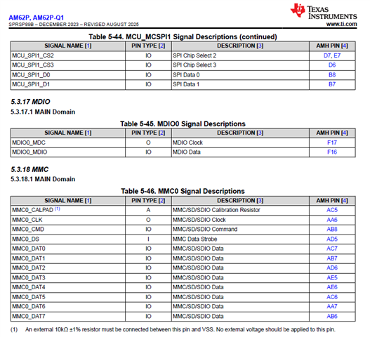
2) We are using the PSE2A0SL-08GX eMMC. This eMMC includes a Data Strobe (DS) pin. Currently, we have connected the DS pin to the W18 pin of the SoC (since it is a free pin, as we are using only a single Ethernet channel). Is this the correct connection? If not, please suggest the proper pin to which it should be connected.

  • Hello Surinder Sharma,

    Thank you for the query.

    We are using the AM620-Q1 EVM reference schematic in our design. In this schematic, there is a net named VPP_LDO_EN which was previously controlled by the I/O expander externally. Now we are not using the I/O expander, where should this signal be connected?

    You can connect to any of the SOC IO that are not used. 

    With the mapping of VPP_LDO_EN to an IO, there will be changes that may be required to be done i the key writer package.

    I understand this is a simple program and allows customer to make the IO mapping changes.

    In case you need support, this is something TI could provide.

    Regards,

    Sreenivasa

  • Hello Surinder Sharma,

    We are using the PSE2A0SL-08GX eMMC. This eMMC includes a Data Strobe (DS) pin. Currently, we have connected the DS pin to the W18 pin of the SoC (since it is a free pin, as we are using only a single Ethernet channel). Is this the correct connection? If not, please suggest the proper pin to which it should be connected.

    Am625 dos not support DS pin.

    You can add a pulldown and a TP as a provision for probing.

    FYI, CALPAD and DS pins are supported on the eMMC hard macro PHY that supports HS400 speed 

    Regards,

    Sreenivasa

  • Hello Surinder Sharma,

    I added the connection recommendations for the change list you shared.

    GPIO_eMMC_RSTn
    Connect to any of the SOC IO to implement local reset.
    In case the IO is different from the one used on the SK (uses IO expander), software changes to remap the IO is required

    This connection is recommended.

    MCU_I2C0
    A pullup is required irrespective of IO usage or configuration

    Add pullup 4.7K for MCU_I2C_ signals
    I2C interface not used
    Open-drain output type buffer I2C interfaces have slew rate requirement when pulled to 3.3 V
    An RC is recommended for slew rate control
    Refer SK-AM62P-LP schematics

    IO_EXP_TEST_LED
    Place pulldown near to pin 3 of FET
    Connect to an SOC IO for indication of 3.3V presence
    This is optional


    GPIO_OLDI_RSTn
    Connect to SOC IO pin for local reset
    Configure the software for the used IO

    CSI_VLDO_SEL
    Connection not visible
    Connect to an SOC IO pin
    Configure the software based on the selected IO

    PORz_OUT Remove shorting from R178 resistor

    Connect an SOC IO with a 10K pullup to one of the ANDing logic input for local reset

    Connect PORz_OUT and RESETSTATz through separate 0R resistors to the other AND gate input.

    Populate 0R for RESETSTATz and DNI series resistor for PORz_OUT initially 

    Regards,

    Sreenivasa

  • In your last comments regarding PORz_OUT and RESETSTATz, both signals are connected to multiple AND gates. Therefore, 0Ω resistor is required for each AND gate, so that we can implement only the ones we need. Is this what you meant? Please confirm. Please share the remaining review points as well, so we can implement them simultaneously.

  • Hello Surinder Sharma,

    In the schematics, there is a 2 input AND gate.

    Please follow below connection.

    Regards,

    Sreenivasa

  • Hello Surinder Sharma,

    I will add the review comments for the first pass review completed schematic, Some additional comments may be added while rerevieing but this should help you with continuing the changes.

    Sree

    Page 3
    reduce R54 value to 22R
    Looks to be a voltage divider now
    Reduce package to 0402 for R54 and R56

    100V cap used for 12V
    Follow below
    100nF/50V/0603

    C136, C137
    10V cap used for 12V supply
    Use 25V or above

    CAN_TX U8
    SOC IO buffers are off during reset
    Add parallel pull in case the input can float
    Suggest adding a pullup

    CAN_VIO_3.3V uC
    Net connection is not visible
    In case this connect to the SOC connection of a large cap load at the output is not allowed or recommended

    BUCK EN CAN
    Net not visible

    Regards

    Sreenivasa

  • Thanks for the comments.

    • CAN_VIO_3.3V uC net is connected to E7 pin of the SoC (Page 20).

    • BUCK EN CAN net is connected to U29 load switch (Page 6).

    This issue occurred due to a PDF generation, while searching for these context.

  • Hello Surinder Sharma,

    Thank you.

    Please refer updated comments 

    CAN_VIO_3.3V uC
    Connected to SOC IO
    Connecting a 100nF cap directly to the SOC output is not recommended
    Reduce the cap value to 22pF
    Move R148 near to the VIO pin5 of U9

    BUCK EN CAN
    Connected to U29 load switch EN
    PMIC GPIO open daring output is also connected.
    SN74AHC1G08 Single 2-Input Positive-AND Gate
    Use a open drain output type AND gate

    Regards,

    Sreenivasa

  • Hi,

    Please explain the BUCK EN CAN connection to U29. Our requirement is that, if in the future we need to control this load switch through the SoC, we should be able to do so.

    Is this suggested by you as per the attached picture?

    Please confirm.

  • Hello Surender

    The above option is Ok but the gate may not be required.

    PMIC GPIO is Open drain output

     SN74AHC1G08 Single 2-Input Positive-AND Gate

    choose below 

    SN74AHC1G09 Single 2–Input Positive-AND Gate With Open-Drain Output

    It is Ok to short 2 open drain outputs and connect a common resistor to perform ANDing. 

     https://e2e.ti.com/support/logic-group/logic/f/logic-forum/865215/faq-with-open-drain-outputs-can-i-use-them-to-shift-a-logic-voltage-level-connect-the-outputs-directly-together-force-a-voltage-node-to-zero 

    With an open-drain output, there is no danger of one output being HIGH and another being LOW since all outputs are either LOW or Hi-Z. In the above image we show how three open-drain buffers can be combined to produce a 3-input AND gate function. It is important to note that the output signal has the same limitation as the previous use-case: the signal can either be fast or low power, but not both.

    Regards,

    Sreenivasa

  • Hi Sir,

    I’m a little confused in this case. Could you please draw the input and output connections of the SN74AHC1G09?