Tool/software:
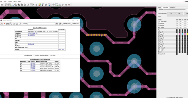
1.In the EVM materials provided, the PCB guide instructs maintaining 66 Ω after the DDR T-branch for impedance. Could you confirm whether we should follow this guideline as-is? The attached image shows 33 Ω, so we’d like to clarify.
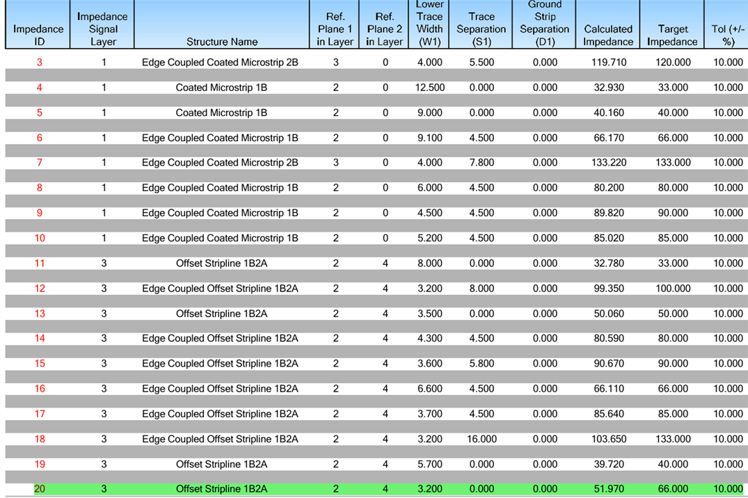
2.Per the stack-up, Impedance ID 20 shows a Layer 3 target of 66 Ω at 3.2 mil width, whereas the calculated value is 51.97 Ω. Was this set to 51.97 Ω because 66 Ω isn’t feasible at 3.2 mil? Also, would proceeding at approximately 50 Ω be acceptable on our side?