AM6442: GPMC_CS interval too long between two access from R5F

Part Number: AM6442

Tool/software:

Hello TI Team,

Processor: AM6442
SDK Version: AM64x MCU+ SDK 11.00.00

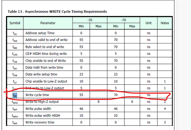
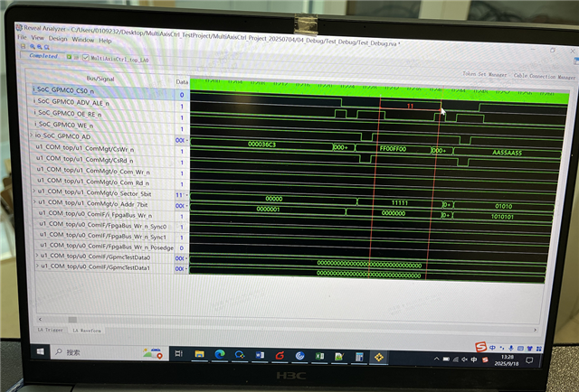
I am currently working with the AM6442 processor on my custom board, focusing on communication between R5F core and RAM through GPMC. When I use asynchronous single-write access on an Address/Data-Multiplexed device, the interval time between two nCS signals(Two writes) is 11 clock cycle(although I have already set the cycle2cycledelay parameters to 2), what parameters can I adjust to reduce the time interval to 2 clock cycles.

Please provide your inputs on this

Thanks and regards

  • Hello ,

    What is the PSRAM size and bits of operation?

    Can you please confirm did you interface the PSRAM or FPGA ?

    If you interface with PSRAM memory, please share the datasheet.

    Please confirm if the timing in between two writes for 11 clock cycles is not meeting the actual throughput ?

    Are you OK going with DMA if you want to improve the throughput?

    Regards,

    Anil.

  • Hello,

    Sorry, we are using FPGA here and do not use wait signal. The following is the relevant configuration information of GMPC in syscfg.

    Chip Select On Time                       1

    Chip Select Read Off Time             10

    Chip Select Write Off Time             10

    ADV On Time                                   2

    ADV Read Off Time                          5

    ADV Write Off Time                           5

    ADV AADMux On Time                     2

    ADV AADMux Read Off Time            5

    ADV AADMux Write Off Time            5

    WE On Time                                      6

    WE Off Time                                      9

    OE On Time                                      6

    OE Off Time                                      9

    OE AADMux On Time                       6

    OE AADMux Off Time                       9

    Page Burst Access Delay                 0

    Read Access Time                            8

    Write Access Time                            9

    Read Cycle Time                              11

    Write Cycle Time                              11

    Write Data AAD Mux Bus Time         5

    Bus Turn Around Time                      0

    Cycle to Cycle Delay                         2

    Cycle Delay Same Chip Select        Add...

    Cycle Delay Different Chip Select    Add...

  • Hello ,

    The above timing information is OK.

    Please provide the answers for all the above queries as well.

    Regards,

    Anil.

  • Hello,

    We use FPGA to mimic NOR FLASH timing. We use 256MB of space and a 32 bit bus, and we do not use WAIT signal and DIR signal. The time interval between two write operations should be reduced to two clock cycles to meet the required throughput.

  • Hello ,

    You cannot force back-to-back single asynchronous write transactions to be only 2 GPMC cycles .
    The controller must wait until the device’s minimum write cycle completes, so your observed ~11 cycles (driver/ADV/address overhead + device min cycle) cannot be compressed to 2 cycles.

    Why 2 cycles is impossible in your setup :
    • PSRAM datasheet gives tWC / tACC ≈ 70 ns. At f_GPMC = 100 MHz a cycle = 10 ns → tWC = 7 cycles.

    The controller cannot start the next write until the current write cycle timing requirement is met.
    • AD-multiplexing (address phase) and small extra CS/WE hold times can add cycles, so seeing 11 cycles is expected. 

    Practical ways to improve overall throughput :
    Use DMA :
    • Throughput gains are large because the per-transaction device timing (tWC) is still required, but you remove CPU inter-write delays and reduce AD/address overhead by doing long contiguous block writes.


    Regards,

    Anil.

  • Hello,

    I apologize for my incorrect expression. The following image is the timing diagram captured during two writes, Now we want to adjust the 11 clock cycles marked between the red lines in the picture.

  • Hi Swargam,

    CYCLE2CYCLEDELAY is 2 FCLK in example.syscfg. But the actual measured time between two read cycle is 11FCLK. Why ?
    I feel like 11FCLK is approximately the read cycle.That is, after a successful read cycle, a read cycle is left empty and nothing is done ?

    GPMC_CONFIG1_i[1-0] GPMCFCLKDIVIDER = 0h GPMC_FCLK frequency
    GPMC_CONFIG1_i[9-8] MUXADDDATA = Address and data multiplexed attached device
    GPMC_CONFIG1_i[13-12] DEVICESIZE = 32bit
    GPMC_CONFIG1_i[28] WRITEMULTIPLE= single access
    GPMC_CONFIG1_i[30] READMULTIPLE = single access

    typedef struct 
    {
        Uint32 ulFpgaRdData[30];
    }FpgaRdParams;
    
    typedef struct
    {
        Uint32 ulFpgaWrData[30];
    }FPGAWrParams;
    
    FpgaRdParams stFpgaRdParamsReg __attribute__((aligned(128), section(".bss.FpgaRd")));
    FPGAWrParams stFPGAWrParamsReg __attribute__((aligned(128), section(".bss.FpgaWr")));
    
    void FPGARead()
    {
        stFpgaRdParamsBuf.ulFpgaRdData[0] = stFpgaRdParamsReg.ulFpgaRdData[0];
        stFpgaRdParamsBuf.ulFpgaRdData[1] = stFpgaRdParamsReg.ulFpgaRdData[1];
    }
    
    void FPGAWrite()
    {
        stFPGAWrParamsReg.ulFpgaWrData[0] = 0xFF00FF00;
        stFPGAWrParamsReg.ulFpgaWrData[1] = 0xAA55AA55;
    }

    Looking forward to your reply !

    Regards,

    Andy

  • Hello Andy/,

    I looked at your your timing cycles, which are OK.

    My observation is that when the R5F core is trying to access the GPMC register it may be to write or read cycle.

    The R5F core can take the 200nsec time.

    So, this time also comes in between two writes or reads.

    What is the GPMC FCLK 100MHZ or 133MHz ?

    Regards,

    Anil.

  • Anil,

    My observation is that when the R5F core is trying to access the GPMC register it may be to write or read cycle.

    It is not accessing GPMC register, it is accessing external FPGA over GPMC in 32bit data/address multiplex mode. 

    What is the GPMC FCLK 100MHZ or 133MHz ?

    133MHz. 

    The timing within one CS is correct according to register configuration. but the interval between to write access is too long, up to 11 GPMC clock cycle.

  • Hello Tony,

    Thank you for sharing the above details.

    Actually, the R5F should access the CS base address for wire and read operations.

    You may be correct that PSRAM memory is memory mapped and not really the R5F core is takes the 0.2usec to access the CS base address .

    I feel that we can do the optimization timing configuration, but the customer is looking forward to why the 11cycles from one CS end to the next CS enable is the question.

    And, cycle 2 cycle delay and the CS to CS delay are one cycle that should be OK.

    I am routing your query to the Hw expert and lets see if he can help here.

    Regards,

    Anil.