


We developed DM8148-based custom hardware.
We need some clarifications about interfacing 16-bit boot NOR flash in A/D mode.
NOR flash is Spansion S29GL01GS12DFIV10 (128 MByte).
The main problem we are facing is that CPU is able to address first 128 kByte of NOR flash only.
The following table summarizes how pin are connected. Lower 16 addresses are latched by 74ALVCH16373 latch driven by GPMC_ADVn_ALE signal.
CPU side (ball) ------- NOR side (ball)
GPMC_D0 (U26) - latch - A0 (E2)
GPMC_D1 (Y28) - latch - A1 (D2)
GPMC_D2 (V27) - latch - A2 (C2)
GPMC_D3 (W27) - latch - A3 (A2)
GPMC_D4 (V26) - latch - A4 (B2)
GPMC_D5 (AA28) - latch - A5 (D3)
GPMC_D6 (U25) - latch - A6(C3)
GPMC_D7 (V25) - latch - A7 (A3)
GPMC_D8 (Y27) - latch - A8 (B6)
GPMC_D9 (AB28) - latch - A9 (A6)
GPMC_D10 (Y26) - latch - A10 (C6)
GPMC_D11 (AA27) - latch - A11 (D6)
GPMC_D12 (U24) - latch - A12 (B7)
GPMC_D13 (U23) - latch - A13 (A7)
GPMC_D14 (V24) - latch - A14 (C7)
GPMC_D15 (Y25) - latch - A15 (D7)
GPMC_A16 (AD27) - NOT CONNECTED
GPMC_A17 (V23) - A16 (E7)
GPMC_A18 (AE28) - A17 (B3)
GPMC_A19 (AC27) - A18 (C4)
GPMC_A20 (AD28) - A19 (D5)
GPMC_A21 (AC28) - A20 (D4)
GPMC_A22 (AB27) - A21 (C5)
GPMC_A23 (AA26) - A22 (B8)
GPMC_A24 (L5) - A23 (C8)
GPMC_A25 (N23) - A24 (F8)
GPMC_A26 (P22) - A25 (G8)
GPMC_A27 (R24) - NOT CONNECTED
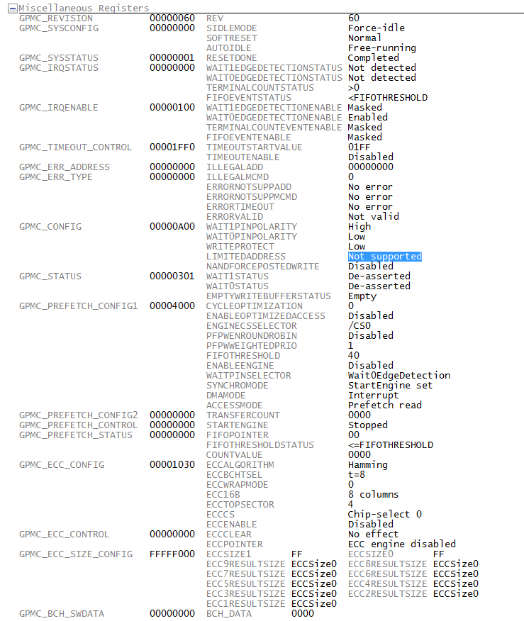
Attached are three images showing some CPU registers at boot:
- Control-Status-Reg-at-boot.png: it shows Control Status Registers
- GPMC-Misc-Regs-at-boot.png: it shows GPMC misc registers
- GPM-CS0-Regs-at-boot.png: it shows GPMC CS0 registers
Referring to Control-Status-Reg-at-boot.png:
ADMUX field of CONTROL_STATUS register is 10b = 2h.
SYSBOOT field of CONTROL_STATUS register is 11010b = 1Ah.
According to TRM sprugz8, this would correspond to the following configuration:
muxing scheme: Addr/Addr/Data Muxing
boot sequence: XIP (MUX0) - UART - SPI - MMC
So muxing scheme seems to be wrong for our NOR connection that is A/D.
However this configuration seems to be correct according to datasheet SPRS647B that says:
BTMODE[14:13] 01b = A/A/D muxed
BTMODE[14:13] 10b = A/D muxed
Our configuration seems to be correct according to section GPMC registers TRM sprugz8 too that says (see GPM-CS0-Regs-at-boot.png):
GPMC_CONFIG1_i.MUXADDDATA = 2h Address and data multiplexed attached device.
As said before, CPU is able to address first 128 kByte of NOR flash only. This is due to the fact that CPU does not move GPMC_A17 and higher address lines that are stuck to 0 even if we try to access area at address 0x0802:0000 and higher. However if we change (via JTAG debugger) field GPMC_CONFIG1_0.MUXADDDATA to 0 (Non-multiplexed attached device), when accessing address 0x0802:0000 CPU moves GPMC_A17 as expected. Thus GPMC_A17 pad has no electrical problems.
So we need to understand:
1) why CPU is unable to address whole flash in A/D mode
2) if our connection scheme is correct
3) which documentation is correct (TRM or datasheet); according to our test, datasheet is correct
4) why CPU moves A17 line only if we select demuxed mode via GPMC configuration register.
Thanks in advance.

