AM67A: QSPI boot

Part Number: AM67A


Tool/software:

Hi,

My customer will try to use QSPI boot (Not OSPI).
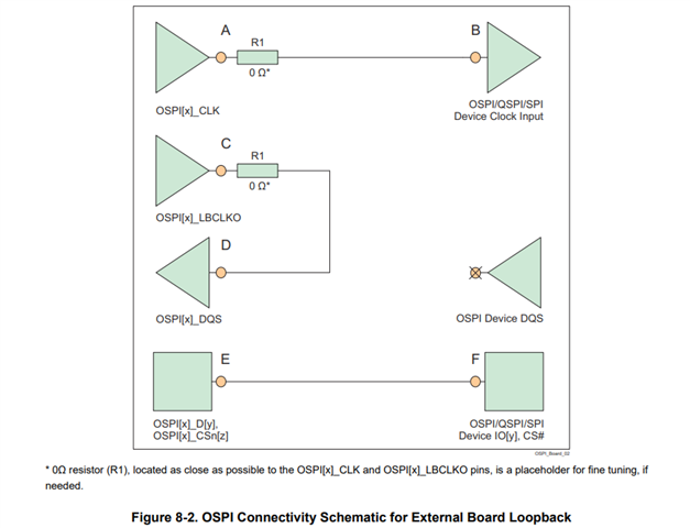
To confirm correct schematic, I'm checking schematic checklist tool as shown below.
https://www.ti.com/jp/lit/an/sprad91b/sprad91b.pdf

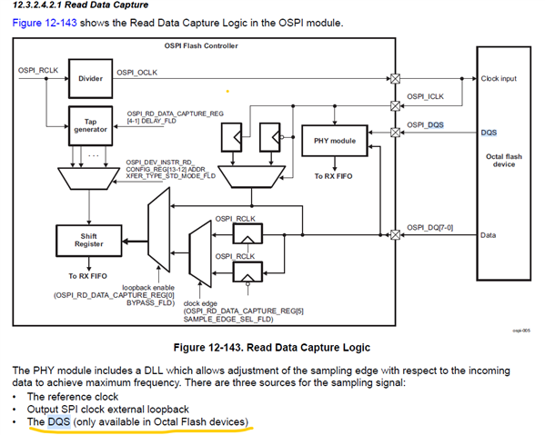
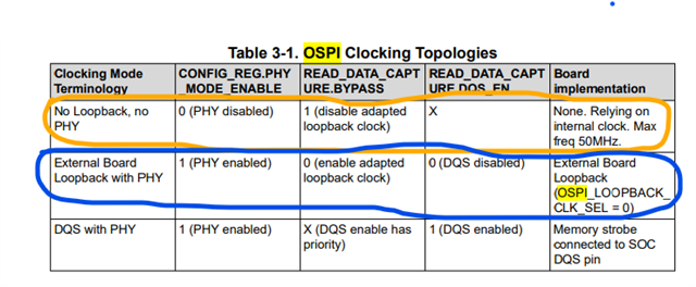
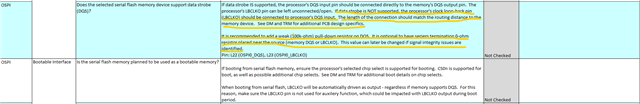
When I check spread sheet, there is following description.

According to this, when user use serial flash for boot, it seems that LBCLKO will be automatically driven as output.
This is defined in "OSPI" column, but is it applied to QSPI as well ?

What kind of output signal is observed on LBCLKO during booting ?

Best Regards,


  • Hello Ryuuichi Machida-san,

    We are currently working through this with the expert. 

    Please ping the thread if you do not get the answers early next week.

    We appreciate your patience !

    Kind Regards,

    Anastas Yordanov

  • Hi Anastas,

    Thank you for your reply.
    I' will wait for your feedback.
    If possible, could you check status of following other stacked thread as well ?

    AM67A: External reference clock requirement for SERDES function - Processors forum - Processors - TI E2E support forums
    AM67A: Trace requirement for PCIe reference clock - Processors forum - Processors - TI E2E support forums

    Best Regards,

  • Hello Ryuuichi Machida-san,

    In the meantime, 

    If possible, could you check status of following other stacked thread as well ?

    I've checked the status as requested. There is already another TI expert assigned to handle the above two threads.

    Thanks

    Kind Regards,

    Anastas Yordanov

  • Hello Ryuuichi Machida-san,

    The section 12.3.2.4.1 Read Data Capture of the AM67A TRM specifies that the DQS pin is not available at the QSPI memory side. 

    For the details of QSPI specific booting, please refer to the section QSPI Boot of the AM67A TRM.

    The section QSPI Bootloader Operation of the AM67A TRM specifies that the quad read speed is 50 MHz. From these sections I understand that TAP (No-PHY) SDR mode is supported by the AM67A RBL QSPI Bootloader. 

    The description of issue i2249 OSPI: Internal PHY Loopback and Internal Pad Loopback clocking modes with DDR timing inoperable .... of the AM67A Silicon Revision 1.0 Errata provides useful info on the working OSPI clock configurations.

    The table under this i2249 note, lists the supported OSPI clocking topologies. For the QSPI flash memory which does not support DQS signal, only the highlighted options shall be valid. The TAP (No-PHY) DDR mode option highlighted in orange shall be valid when the AM67A ROM performs booting from the QSPI memory. The External Board Loopback with PHY topology is used to allow faster operations of QSPI  (custom bootloader or other operations with Flash memory). 

    The two connectivity corresponding configurations are illustrated in the Section,  No Loopback, Internal PHY Loopback, and Internal Pad Loopback and Section, External Board Loopback of the Device Datasheet

    As I refer to the schematic checklist tool from the: https://www.ti.com/jp/lit/an/sprad91b/sprad91b.pdf that you pointed, there is also another note which specifies the connectivity in case that data strobe output (DQS) not available from memory side. Please refer to the guidelines highlighted in yellow. According to the guideline the LBCLKO output shall be connected to the DQS input.  

     I hope these findings answer your questions.

    Thanks

    Kind Regards

    Anastas Yordanov

  • Hi,

    Thank you for your reply.

    As I refer to the schematic checklist tool from the: https://www.ti.com/jp/lit/an/sprad91b/sprad91b.pdf that you pointed, there is also another note which specifies the connectivity in case that data strobe output (DQS) not available from memory side. Please refer to the guidelines highlighted in yellow. According to the guideline the LBCLKO output shall be connected to the DQS input.  

    What I would like you to confirm is whether above content should be applied to QSPI as well.
    Is my understanding that user should follow above content to case of QSPI correct ?

    Best Regards,

  • Hello Ryuuichi Machida-san,

    I will refer your request for confirmation to a TI expert. Please expect one to two days delay in response.

    Thanks for your patience !

    Best Regards

    Anastas Yordanov

  • Hi,

    I re-read contents of TRM.
    Actually, it seems that LBCLKO is NOT used case of QSPI boot.
    So, I understood that user can not follow checklist of case of OSP for treatment of LBCLKO, however could you confirm this just in case ?

    Best regards, 

  • Hello Ryuuichi Machida-san,

    I already referred your question to our OSPI/QSPI expert as promised.

    However I am still waiting for his confirmation. Once it is confirmed I will let you know.

    Thanks for your understanding !

    Kind Regards,

    Anastas Yordanov

  • Hello Ryuuichi Machida-san,

    I would like to apologize for the delay in my response !

    I got confirmation from the OSPI/QSPI expert:

    Even in the case when DQS output does not exist on the serial flash memory side, as its the case with the QSPI memory, looping back OSPI_LBCLK0 to OSPI_DQS at the AM67A SoC side helps close timing on higher speeds. Therefore it is recommended that the SoC OSPI_LBCLKO pin is connected  to the OSPI_DQS pin of the SoC for QSPI serial flash memories as well. 

    Make sure that the hardware connection OSPI_LBCLKO to OSPI_DQS at the AM67A SoC side follows the specific PCB trace + pull-down resistor requirement as per the AM6x_TDA4x_DRA8x_SchemCheckList_Tool_v2.02.0.xlsm and also the guidance provided in the the Subsection, External Board Loopback of the Section, OSPI/QSPI/SPI Board Design and Layout Guidelines of the AM62A7 Datasheet. I had confirmation from the expert that the connectivity diagrams and layout / signal integrity guidance in the section OSPI/QSPI/SPI Board Design and Layout Guidelines of the AM67A DS are valid for the QSPI flash memories too.

    Does this clarify your questions ? Let me know.

    Thanks for your patience once again !

    Kind Regards,

    Anastas Yordanov

  • Hi,

    Thank you for your reply.

    Even in the case when DQS output does not exist on the serial flash memory side, as its the case with the QSPI memory, looping back OSPI_LBCLK0 to OSPI_DQS at the AM67A SoC side helps close timing on higher speeds. Therefore it is recommended that the SoC OSPI_LBCLKO pin is connected  to the OSPI_DQS pin of the SoC for QSPI serial flash memories as well. 
    => Currently, customer do NOT connect LBCLKO to DQS. According to description of "looping back OSPI_LBCLK0 to OSPI_DQS at the AM67A SoC side helps close timing on higher speeds.",  it seems that connection between LBCLKO and DQS when user use QSPI is NOT mandatory.
    Is my understanding correct ?

    Best Regards,

  • Hi,

    Additionally, I would like to confirm about below.
    Could you please give your comment about below as well ?

    * As I described previous thread, I understand that "OSPI_LBCLK0" and "OSPI_DQS" are NOT active when user use QSPI boot.
    So, I'm not sure why connection between LBCLK0 and DQS will help timing.
    If possible, could you please show the reason about above ?

    Best Regards, 

  • Hi Ryuuichi Machida-san,

    The expert told me, even when RBL/ROM bootloader boots over QSPI you should see output clock at the OSPI_LBCLKO. His recommendation for the customer is to connect the loopback LBCLK0 pin to the DQS pin and follow the guidance provided in the AM6x_TDA4x_DRA8x_SchemCheckList_Tool_v2.02.0.xlsm and in the  datasheet - the Section, OSPI/QSPI/SPI Board Design and Layout Guidelines of the AM62A7 Datasheet. 

    Q1: Is the LBCLKO to DQS connection missing in the production layout ?

    Q2: Is the boot from QSPI successful ?

    Q3: What is the maximum OSPI_CLK during QSPI reads that is obtained without this connection (PHY disabled) ?

    Thanks

    Kind Regards,

    Anastas Yordanov

  • Hi,

    Q1: Is the LBCLKO to DQS connection missing in the production layout ?
    Q2: Is the boot from QSPI successful ?
    Q3: What is the maximum OSPI_CLK during QSPI reads that is obtained without this connection (PHY disabled) ?
    => Now, they are developing stage. So they do not have production layout yet.
    However, they use several function and uart function have already been assigned to LBCLK and DQS pin.
    So, if this change is necessary, they need to confirm whether they can move layout and re-assign uart function to another pins.

    Best Regards,

  • Hi Ryuuichi Machida-san,

    Thank you for the clarification. 

    I need a bit more information regarding the usecases for this QSPI flash memory:

    Q1. Is this a QSPI NAND/ NOR flash memory ? If NOR, does it support XIP mode ?

    Q2. Would be the AM67A OSPI interface used only for booting from the QSPI memory ?

    Q3. What maximum transfer frequency is expected for customer bootloaders booting ?

    Q4. Do you intend to load any applications and data to RAM from the QSPI memory ? If yes what transfer speed is expected ?

    Thanks

    Kind Regards,

    Anastas Yordanov

  • Hi,

    Q1. Is this a QSPI NAND/ NOR flash memory ? If NOR, does it support XIP mode ?
    => Customer will use NOR flash with supporting XIP mode.

    I will confirm customer about remaining questions(Q2 - Q4). Please wait my feedback.

    Best Regards,

  • Hi,

    Here are answers for remaining questions.

    Q2. Would be the AM67A OSPI interface used only for booting from the QSPI memory ?
    => Basically, customer will use QSPI memory as dedicated boot memory. However, customer is considering following thing except booting.
    1. Write start-up log. (small amount)
    2. Change boot loader from Linux kernel.

    Q3. What maximum transfer frequency is expected for customer bootloaders booting ?
    => They will plan to set 20Mhz as QSPI clock.
    (However, they do not need to set such clock speed. So if requirement of threshold for external loopback(LBCLKO to DQS) is less than 20MHz, they may be able to change lower clock speed.

    Q4. Do you intend to load any applications and data to RAM from the QSPI memory ? If yes what transfer speed is expected ?
    => They have another memory for application.

    Best Regards,


  • Hello Ryuuichi Machida-san,

    Please consider that OSPI_CLK with frequency <=20 MHz is NOT supported by the AM67A ROM bootloader when booting from a QSPI memory. Also xSPI mode will be unsupported by the AM67A ROM bootloader.

    These are covered in the Section, Initialization / Subsection, QSPI Boot of the AM67A TRM

    Please consider the above restrictions if the customer would like to have option for AM67A ROM booting from the QSPI NOR Flash.

    And I have sent a query to the ROM Bootloader team to check if 50 MHz booting is supported without an external Board loopback connectivity between the OSPI0_LOOPBACK pin and the OSPI0_DQS pin.

    I would also request confirmation if the QSPI controller will be able to support:

    A/ transfers that feature <=20MHz

    B/ QSPI memory XIP mode with frequency <= 20MHz

    without OSPI0_LOOPBACK pin connectivity to the OSPI0_DQS pin.  

    Thanks for your patience once again !

    Kind Regards,

    Anastas Yordanov

  • Hi

    >Please consider that OSPI_CLK with frequency <=20 MHz is NOT supported by the AM67A ROM bootloader when booting from a QSPI memory.
    => I believe that this is default setting on ROM bootloader.
    After moving boot sequence to secondary bootloader, we can change spi clock.
    I thought that what you ask is above setting of secondiary bootloader(or kernel setting).
    Is my understanding incorrect ?

    >And I have sent a query to the ROM Bootloader team to check if 50 MHz booting is supported without an external Board loopback connectivity between the OSPI0_LOOPBACK pin and the OSPI0_DQS pin.
    >I would also request confirmation if the QSPI controller will be able to support:
    => Thank you for your confirmation.
    Deadline of schmatic/layout is coming up soon, so I hope your quick reply as possible as you can.

    Best Regards,

  • Hello Ryuuichi Machida-san,

    I thought that what you ask is above setting of secondiary bootloader(or kernel setting).
    Is my understanding incorrect ?

    I actually already understood that customer would like to have their secondary bootloader (SBL) booting other custom bootloaders or Linux applications  from the QSPI NOR flash using OSPI0_CLK freq <=20MHz . I just wanted to remind the customer that the default AM67A ROM loader booting frequency is (50MHz) in QSPI boot mode. As you already mentioned, as a workaround, the customer SBL (secondary bootloader) can later switch the QSPI memory clock to <=20MHz when control passed to it by the AM67A  ROM bootloader.  

    There is a still my ongoing discussion with the experts regarding the accurate OSPI mode (TAP / PHY  vs frequency) in which QSPI memory will be able to work reliably at 50 MHz and <=20 MHz without the external loopback from the SoC LBCLKO output  pin to the SoC DQS input pin.

    I'll take into consideration your project schedule as much as I can. I hope we clarify this until tomorrow EOB.

    Sorry for the inconvenience !

    Thanks

    Kind Regards,

    Anastas Yordanov   

  • Hello Ryuuichi Machida-san,

    For now I have a confirmation by the TI AM67A ROM team that the ROM bootloader will set the OSPI controller in TAP SDR mode (using 50MHz OSPI_CLK to the QSPI memory) when booting from the customer QSPI Flash memory. With Tap mode there is no need of a loopback, and this has been validated without connection from LBCLKO to DQS pin. The OSPI internal reference clock RCLK will be set to 200 MHz by the ROM, to derive 200/4 = 50 MHz.  As we already know from the TRM, the ROM QSPI boot is not a XIP boot.

    I am still expecting AM67A team feedback to confirm on the <=20 MHz, no loopback, QSPI memory boot and other usage scenarios !

    Thanks

    Kind Regards 

    Anastas Yordanov