


Tool/software:
I am working on a custom design, and looking at reference design PROC114E3. I am using a similar DDR4 memory IC.
I have reviewed to document, and the schematic and I am trying to piece a few things together.
Looking at sprad06c.
As I understand it, the DDR4 memory has defined net class and signals.
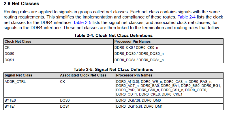
My interpretation is that the ADDR_CTRL lines shown should length match the CK lines shown.
Additionally, these should length match to the farther possible reach. The guide references that A13 may be the farthest.
However, based on the IC orientation of PROC1143E, the two CK pins are the farthest away from the processor.
The routing guidelines gives max delay times.
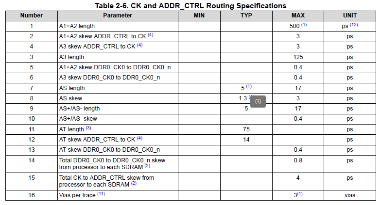
And it states: To use length matching (in mils) instead of time delay (in ps), multiply the time delay (in ps) limit by 5.
The address lines can be up to 2500 mils.
When I review the design mentioned, the two clock lines are ran with a length of 1492 mils each.
I read Line 2 above that the skew between ADDR and CK needs to be 3ps, or 15 mils.
But when I look at the address lines they do not match the clock lines, not are they within 15mils (3ps) of the clock lines.
A0: 1392 mils
A1: 1391 mils
...
A13: 1395 mils
The other items in table 2-5 are not quite the same either:
BA0: 1316 mils
BA1: 1316 mils
ODT: 1296 mils
What am I misunderstanding?
