TDA4VH-Q1: Information on pin R29 of SoC (VCM)

Part Number: TDA4VH-Q1
Other Parts Discussed in Thread: OPA365-Q1

Tool/software:

Hi TI team,

I am working on VCM with Khemraj,

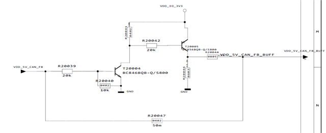
In our design we have implemented voltage monitor ckt at pin R29 pin of  at SoC(TDA4VH88T5AALYRQ1) for monitoring 5V using external voltage divider as shown in below image.

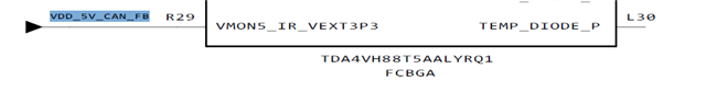
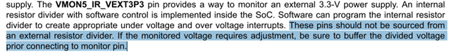
In datasheet  for R29(VMON5_IR_VEXT3P3) its mentioned that :

1.) Its shouldn't be provided from external divider and if its provided then need to buffer the divided voltage.

----> Q-1) Is the provided configuration OK, or will it have issues?

The voltage divider network is provided with 5V,that will generate 3.516V which is under the pin max voltage limit (-0.3 to 3.8V)

---->Q-2)  During transient conditions or in case of an operational fault, Input voltage to resistor divider rail may rise to 6 V instead of the nominal 5 V. Under such a condition, the current voltage divider configuration would output 4.219 V, which exceeds the maximum allowable voltage at the SoC pin.

If the SoC pin experiences 4.219 V, will it potentially damage the SoC pin, or is there any internal protection mechanism that would detect the over-voltage condition and transition the SoC into a cutoff or safe mode?

Please confirm if the configuration is OK, or do we need to change the resistor divider?

  • Below is snip-it from processor data manual:

    #1:  As stated, VMON5 input should NOT be connected directly to external resistor divider.  If external voltage adjustment is needed, recommendation is to buffer the divider voltage.

    #2:  As stated in data manual, absolute max voltage on pin is 3.8V.  Anything above this voltage could potentially damage the device.

  • Hello Robert,

    Thanks for the quick feedback

    As per your feedback and datasheet it mentioned for R29(VMON5_IR_VEXT3P3) is,

    1.) Its shouldn't be provided from external divider and if its provided then need to buffer the divided voltage.

    ----> Q-1) In our design external voltage divider is need is must because we cannot give 5V directly otherwise pin gets damage, and If we use divider then buffer is must so can you please suggest what kind of buffer we can use or any suggested part number would be helpful.

    2.) Software can program the internal resistor divider to create appropriate under voltage and over voltage interrupts.

    ----> As per our requirement , default voltage at VDD_5V_CAN is 5V and as per voltage divider design it will generate 3.516V which is under the pin max voltage limit (-0.3 to 3.8V)

           Q-2) Can we treat 3.516 V (the divider output at 5 V) as the reference for SW-programmed under/over thresholds, or must we redesign the divider to output 3.3 V nominal so thresholds map to standard 3.3 V?

    ----> During transient conditions or in case of an operational fault, the VDD_5V_CAN rail may rise to 6 V instead of the nominal 5 V. Under such a condition, the current voltage divider configuration would output 4.219 V, which exceeds the maximum allowable voltage at the SoC pin.

          If the SoC pin experiences 4.219 V, will it potentially damage the SoC pin as you mentioned and information provided in datasheet So can you provide possible solution for this scenario, I have a approach in mind if its possible I'm describing it below


    ** Possible solution**


    ----> Q-4) If we design in such a way that when 6V will come at VDD_5V_CAN then at resistor divider provide 3.3V and when 5V will come at VDD_5V_CAN rail then voltage divider generate some X volt which is less then 3.3V, but SoC will have to continuous monitor this X voltage even its not 3.3V  is this approach acceptable?

  • Regarding the buffer suggestion - consider using op-amp (example OPA365-Q1) with a gain of one.  No special requirements, so most any op-amp selection should be possible.

    Regarding the 6V spike, can you use a diode to clamp the voltage (with resistor to limit the current)?

    Regarding the software programmability, below is some information.  For the 3P3 monitor, the voltage steps are 0.0375V

  • Hello Robert,

    Thanks for the response and sorry for the late replay,

    Currently we came up with a plan to add buffer with PNP and NPN combination I hope this will work correct?

    or any other CKT needs to be add?

  • I don't have any additional feedback on this topic.  Do you have any additional questions?