This thread has been locked.

If you have a related question, please click the "Ask a related question" button in the top right corner. The newly created question will be automatically linked to this question.

AM5726: Problem with QSPI interface

Part Number: AM5726
Other Parts Discussed in Thread: TPS659037

We have connected a QSPI flash to the AM5726 processor according to the picture.

QSPI.PNG


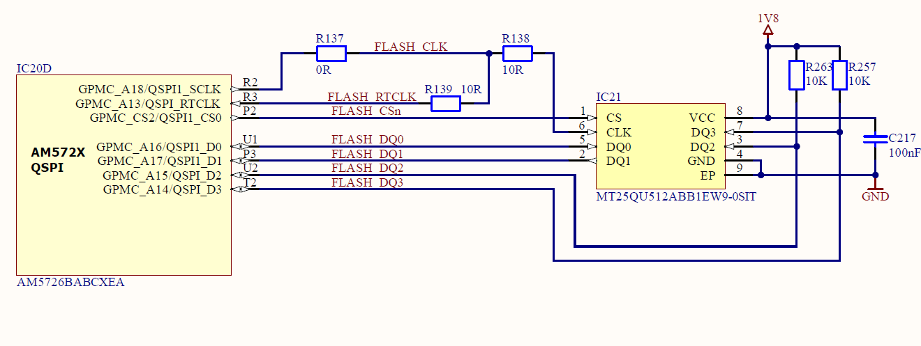
The bank power supply for all these pins is corrcet (1.8V) The communication is not stable. Also with the oscilloscop. It looks as if the RTCLK input is not a input. 

For testing we put all these pins into simple GPIO mode. Also with R139=150 Ohm The RTCLK input pin falsies the SCLK output signal. 

What is wrong with these "input" pins? Do we have a hardware corruption? Why?

This is the signal at the RTLK "input" (blue) pin when toggeling SCLK (violet). Also as stupid IO.


tek00004.png

  • Some clarification (I'm in the same group as Christoph Stiebel):

    Basically we isolated the sclk pin (R2) and the rtclk pin (R3) by a 150 Ohms resistor to study the (unintended) currents flowing between the pins. The flash is not connected (R138 removed). We programmed sclk as gpio_2_8 output and made it generate a square signal (gpioset -t1us,1us -c gpiochip3 8=1 under linux). The rtclk pin is programmed as gpio_2_3 input. While the voltage at the output gpio2_8 is a good square wave with levels of 1.76V (high) and 0.1V(directly after the falling edge) we observe a falling edge to about 0.6V on the gpio2_3 input which falls (smoothly) to 0V after an arbitrary time ranging from some ns to  some us. From the voltage drop on the 150 Ohm resistor we conclude that the gpio2_3 input is sinking 1.3mA on the 1.8V high level and sourcing 3.3mA on the low level, directly after the falling edge.


    The above oscilloscope screenshots show the situation on the gpio2_8 (output), yellow and the gpio2_3 input (white) on 2 different time scales. The probe is a passive x20 low capacity probe with 1k/1.5pF, so no serious load. The behaviour depends also from the chip temperature: if cool it's rather like on the picture of my colleague (blue trace), if hot, rather like on the white/yellow trace pictures.

    The effect stays the same if we program gpio2_3 as output and gpio2_8 as input, just both traces are swapped (Still clean signal at output, bad signal at input).

    In qspi operation we have indications that also the qspi data io's have the same malfunction when they operate as inputs as the responses of the flash are also corrupted. Especally the low level is forced (by the input pin sourcing a current) in the range of 0.6V making the signalling unreliable.

    What could be the reason????

  • Hi Christoph S. and Christoph D.,

    Do you see similar issues on a secondary or additional boards?

    Can you please also provide the pad configuration for both pins?

  • We encounter the same issue on all specimens of our board (we have 5 pieces).

    In the meantime we also saw it work correctly with the same software, (in that case the inputs are real inputs without temporary load and if we enable and use qspi everything works as expected) but rarely. It seems to be a startup issue and we are thinking in the direction of the power sequencing...

    We have vddshv10 and vddshv11 supplied with 1.8V and tied to vdds18v as permitted in SPRS593G, page195, note (6). vddshv10 supplies the qspi pins. The other vddshv (1-7,9) are 3.3V, enabled later as descrbed on p194. Can this be a problem? (Inother words is it permissible to supply vddshv10,11 on startup with 1.8V and the other vddshv later?


    All reference schematics that we find on the internet have all vddshv supplied with the same 3.3V... I hope, the powering up with 2 different io voltages at different times is not problematic (though the datasheet does not forbid it...). The pad configuration for both pins (R2, R3)was 14 (gpio) for the screenshots above and 1 in qspi mode. in both modes, there is the same effect that the input sources a rather strong current.

  • Hi Christoph D.,

    Thank you for confirming this issue is seen on 5/5 boards using the same software. I share your interpretation of the power sequencing requirement for the VDDSHV10/11 tied to VDDS18V—this is okay. Just for confirmation, is the power solution using the TPS659037 PMIC?

    Can you please share the full pad configuration register? While I recognize the system intermittently works with the same software, I would like to confirm these register values to rule out any configuration issues.

  • Yes the power solution is TPS6590379 PMIC, see below

    During the gpio test (oscilloscope pics) the R2 padconfig (gpmc_a18, addr 0x4A003488) as well as R3 padconfig (gpmc_a13,0xa003474) are both 0x0005000E (read out with devmem2) 

    Please find below the schematic of our power supply. 5V comes first, then 3V3_pre is generated externally. The PMIC switches  on 3V3 via IC11 through REGEN1.

    By the way, for the high output level everything is ok. The slight drop of the white trace (measured at the gpio2_3 input) compared to the yellow trace (gpio2_8 output) at high level comes from the low 1kOhm impedance of the oscilloscope probe generating this drop on the 150 Ohm resistor after the output. The chip was also very hot. When cooled to normal operating temperature and with normal 1M oscilloscope probes the situation looks rather like in the first picture (output in purple, input blue)

  • The schematics show R139 populated with a 10-ohm resistor, but comments state its populated with 150-ohm resistor.  The waveforms showing are with which configuration?  Also I see the blue toggling but the violet not toggling - so what is causing blue to toggle if violet is not (isn't violet the source)?  How is the implemented on the PCB?  Note our datasheet recommend the below:

  • Originally it was populated with a 10 Ohm resistor, exactly as in your recommendation. When the qspi flash was not working properly (ID readout failed) we were examining the signals and saw problems with the signals reaching proper low levels (sometimes more than 0.6V, causing the qspi malfunction). In order to examine more closely we replaced the 10Ohm  R139 (or R2 in your schematic) with a 150Ohm resistor, not to make qspi work but to prove the theory that current was coming out of the input pad.  To make the experiment we also switched the pad functions from qspi to gpio to generate a square output on pad R2. R3 is confiured as an input. And we can observe indeed that the input pad sources current for up to 900ns after it receives the falling edge. Directly at the input we see a level of 0.8V after the falling edge, whereas the output (R2) is rather clean (though you also see a small influence (0.2V), small due to the low output impedance). This shows that for up to 900ns the input pin R3 sources a current of (0.8V-0.2V)/150Ohm = 4mA during a certain time. This seems a malfunction of the pad driver. In rare cases, the bord powers up and works, the voltage at the input (and output) then go down to 0V very cleanly indicating that there is no current sourced by the input. if the board wakes up in "ok" mode it stays ok until the next power up. 

    The same effect can also be observed with other pins of the qspi interface (eg on D1, the flash can't pull down the D1 line properly to 0V)

  • Thanks for the description.  So this is not a signal integrity issue you are investigating but more of a IO functionality issue.  Is that correct?

    In previous comments you mentioned power sequencing issues?  Are you violating the power sequence requirements?

    Another thought - the device has internal pull resistors that can be enabled.  Could this be what you are seeing?

    Note this device has been in production for many years and most customers use the QSPI interface a a primary flash device. I'm not aware of any issues.

  • Robert,

    Based on their provided pad configuration register value, the internal pull resistors are disabled (bit 16 set high).

  • Christoph D.,

    Considering we're running into issues with QSPI, can we please confirm which mode the QSPI is in by dumping QSPI_SPI_DC_REG (0x4B300044)?

    We would want to ensure we're in Mode 0 for the external loopback mode.

  • Dear Mark and Robert. We fully trust TI that the device is not buggy. Therefore we search the bug on our side, e.g a power-up sequence issue. While there is no obvious violation in the power-up sequence (this we chacked first), the data sheet lets some room for interpretation, see above our question if it is permitted to have 1.8V on vddshv10,11 rising together with vdds18 and 3.3V on the other vddshv, rising later.

    And it's not a (timing) signal integrity issue but a voltage level signal integrity issue caused by the IO-Pad behaviour in input mode.

    We did the QSPI test in mode 3 AND in mode 0. If the device powers up correctly, BOTH modes work like a charm, even up to 76.8MHz (Though this is nearly double the sepcified max for mode 3). This proves (together with high-speed oscilloscope measurements) that there is no timing signal integrity issue. Instead we see this strange current sourcing (4mA) from input pins (as well rtslk as data pins) that ceases some ns to some 100 of ns after the falling edge. It looks as if the input would be in a kind of (strong) bus hold mode. I'll do more measurements with different resistors in front of the input to better characterise the current sourcing behaviour. 

  • Dear Mark and Robert. The issue is solved.The cause were 2 3V3 powered inputs of the AM5726 (UART3_RXD, D27 and erroneously also RSTOUTn, F23) that were driven by peripheral circuits powered by 3V3_pre. As the peripherals were driving a high level during startup on the inputs before even vdd18s was applied to the processor there was significant current (estimated 20mA) flowing into these pins during startup. This current flow was apparently able to bring the inputs on vddshv10,11 into this strange state. Now we made sure that these peripherals are also powered by the late 3V3 of the processor and as well our squarewave test as also the whole qspi interface come up reliably. here some screen shots:


    square gpio test  not working                                 /                    working


    qspi flash probe (mode 3) (blue: clock; purple: flash do) not working   /                          working

    I hope the result might be useful to somebody else.

    Thank you for your support!!

  • Glad to hear it's working and thanks for reporting back on this thread!